
Instruction Manual

CS5461A
24 DS661F3
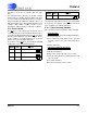
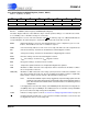
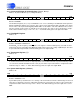
5.14.5 Register Read/Write
The Read/Write informs the command decoder that a register access is required. During a read operation, the ad-
dressed register is loaded into an output buffer and clocked out by SCLK. During a write operation, the data is
clocked into an input buffer and transferred to the addressed register upon completion of the 24
th
SCLK.
W/R
Write/Read control
0 = Read
1 = Write
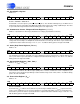
RA[4:0] Register address bits (bits 5 through 1) of the read/write command.
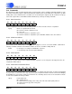
Address
RA[4:0] Name Description
0 00000 Config Configuration
1 00001 I
DCoff Current DC Offset
2 00010 I
gn Current Gain
3 00011 V
DCoff Voltage DC Offset
4 00100 V
gn Voltage Gain
5 00101 Cycle Count Number of A/D conversions used in one computation cycle (N)).
6 00110 PulseRateE
1,2
Sets the E1 and E2 energy-to-frequency output pulse rate.
7 00111 I Instantaneous Current
8 01000 V Instantaneous Voltage
9 01001 P Instantaneous Power
10 01010 P
Active Active (Real) Power
11 01011 I
RMS
RMS Current
12 01100 V
RMS
RMS Voltage
14 01110 P
off Power Offset
15 01111 Status Status
16 10000 I
ACoff Current AC (RMS) Offset
17 10001 V
ACoff Voltage AC (RMS) Offset
18 10010 PulseRateE
3
Sets the E3 energy-to-frequency output pulse rate.
19 10011 T Temperature
20 10100 SYS
Gain
System Gain
21 10101 PW Pulse width register for mechanical counter output mode
22 10110 PulseWidth Pulse width register for E3
energy pulse output
23 10111 VSAG
Duration Voltage Sag Duration
24 11000 VSAG
Level Voltage Sag Level Threshold
25 11001 LoadIntv No load threshold interval (detection window)
26 11010 Mask Interrupt Mask
27 11011 LoadMin No Load Threshold
28 11100 Ctrl Control
29 11101 T
Gain
Temperature Sensor Gain
30 11110 T
off
Temperature Sensor Offset
31 11111 S Apparent Power
Note: For proper operation, do not attempt to write to unspecified registers.
B7 B6 B5 B4 B3 B2 B1 B0
0W/R
RA4 RA3 RA2 RA1 RA0 0