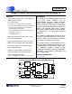
CS5461A Single Phase, Bi-directional Power/Energy IC Features Description • Energy Data Linearity: ±0.1% of Reading over 1000:1 Dynamic Range The CS5461A is an integrated power measurement device which combines two analog-to-digital converters, power calculation • On-chip Functions: engine, energy-to-frequency converter, and a - Instantaneous Voltage, Current, and Power serial interface on a single chip.
CS5461A TABLE OF CONTENTS 1. Overview . . . . . . . . . . . . . . . . . . . . . . . . . . . . . . . . . . . . . . . . . . . . . . . . . . . . . . . . . . . . . . . .5 2. Pin Description . . . . . . . . . . . . . . . . . . . . . . . . . . . . . . . . . . . . . . . . . . . . . . . . . . . . . . . . . . .6 3. Characteristics & Specifications . . . . . . . . . . . . . . . . . . . . . . . . . . . . . . . . . . . . . . . . . . . . .7 Recommended Operating Conditions . . . . . . . . . . . . . . . . . . . . . . . .
CS5461A 6.3 Current and Voltage Gain Register ( Ign ,Vgn ) . . . . . . . . . . . . . . . . . . . . . . . . . . . . 27 6.4 Cycle Count Register . . . . . . . . . . . . . . . . . . . . . . . . . . . . . . . . . . . . . . . . . . . . . . . . 27 6.5 PulseRateE1,2 Register . . . . . . . . . . . . . . . . . . . . . . . . . . . . . . . . . . . . . . . . . . . . . . 28 6.6 Instantaneous Current, Voltage and Power Registers ( I , V , P ) . . . . . . . . . . . . . . 28 6.7 Active (Real) Power Registers ( PActive ) .
CS5461A LIST OF FIGURES Figure 1. CS5461A Read and Write Timing Diagrams ........................................................................... 11 Figure 2. Data Flow. ................................................................................................................................ 13 Figure 3. Normal Format on pulse outputs E1 and E2............................................................................ 16 Figure 4. Alternate Pulse Format on E1 and E2 ...............................
CS5461A 1. OVERVIEW The CS5461A is a CMOS monolithic power measurement device with a computation engine and an energy-to-frequency pulse output. The CS5461A combines a programmable-gain amplifier, two analog-to-digital converters (ADCs), system calibration and a computation engine on a single chip.
CS5461A 2.
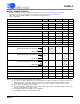
CS5461A 3. CHARACTERISTICS & SPECIFICATIONS RECOMMENDED OPERATING CONDITIONS Parameter Positive Digital Power Supply Positive Analog Power Supply Voltage Reference Specified Temperature Range Symbol VD+ VA+ VREFIN TA Min 3.135 4.75 -40 Typ 5.0 5.0 2.5 - Max 5.25 5.25 +85 Unit V V V °C ANALOG CHARACTERISTICS • • • • Min / Max characteristics and specifications are guaranteed over all Recommended Operating Conditions.
CS5461A ANALOG CHARACTERISTICS (Continued) Parameter Symbol Min Typ Max Unit T - ±5 - °C PSCA PSCD PSCD - 1.1 2.9 1.7 - mA mA mA PC - 21 12 8 10 28 16.5 - mW mW mW µW 45 70 2.3 - 65 75 2.45 2.55 2.7 dB dB V V Temperature Channel Temperature Accuracy Power Supplies Power Supply Currents (Active State) IA+ ID+ (VA+ = VD+ = 5 V) ID+ (VA+ = 5 V, VD+ = 3.3 V) Power Consumption Active State (VA+ = VD+ = 5 V) (Note 3) Active State (VA+ = 5 V, VD+ = 3.
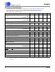
CS5461A DIGITAL CHARACTERISTICS • • • • Min / Max characteristics and specifications are guaranteed over all Recommended Operating Conditions. Typical characteristics and specifications are measured at nominal supply voltages and TA = 25 °C. VA+ = VD+ = 5V ±5%; AGND = DGND = 0 V. All voltages with respect to 0 V. MCLK = 4.096 MHz. Parameter Symbol Min Typ Max Unit 2.5 4.
CS5461A SWITCHING CHARACTERISTICS • • • • Min / Max characteristics and specifications are guaranteed over all Recommended Operating Conditions. Typical characteristics and specifications are measured at nominal supply voltages and TA = 25 °C. VA+ = 5 V ±5% VD+ = 3.3 V ±5% or 5 V ±5%; AGND = DGND = 0 V. All voltages with respect to 0 V. Logic Levels: Logic 0 = 0 V, Logic 1 = VD+.
CS5461A t3 CS t1 t2 SC LK H ig h B y te LSB MSB MSB-1 LSB MSB LSB MSB C o m m a n d T im e 8 S C L K s MSB-1 t5 MSB-1 LSB MSB SDI MSB-1 t4 M id B y te L o w B y te SDI Write Timing (Not to Scale) CS t1 t8 LSB MSB-1 LSB MSB L o w B y te MSB-1 LSB UNKNOW N MSB-1 MSB SDO M id B y te MSB H ig h B y te t6 t7 t2 LSB MSB-1 SDI MSB SC LK C o m m a n d T im e 8 S C L K s SYN C 0 or SYN C 1 C om m and SYN C 0 or SYN C1 C om m and SYN C 0 or SYN C1 C om m and SDO Read
CS5461A ABSOLUTE MAXIMUM RATINGS WARNING: Operation at or beyond these limits may result in permanent damage to the device. Normal operation is not guaranteed at these extremes. Parameter DC Power Supplies Input Current, Any Pin Except Supplies Symbol Min Typ Max Unit (Notes 18 and 19) Positive Digital Positive Analog VD+ VA+ -0.3 -0.3 - +6.0 +6.
CS5461A VDCoff* Vgn * VACoff* V* Digital Filter VOLTAGE x10 2nd Order Modulator DELAY REG SINC 3 X IIR HPF Option + + X APF Option 6 N X Poff * PulseRateE1,2 * ÷N X + PC6 PC5 PC4 PC3 PC2 PC1 PC0 SYSGain * X Configuration Register * + P* APF Option CURRENT PGA 4th Order Modulator SINC 3 DELAY REG X IIR HPF Option Digital Filter + N PulseRateE 3 * N X X + IDCoff* I gn* * DENOTES REGISTER NAME.
CS5461A To generate a value for the accumulated active energy over the last computation cycle, the active power can be multiplied by the time duration of the computation cycle. The apparent power is the combination of the active power and reactive power, without reference to an impedance phase angle, and is calculated by the CS5461A using the following formula: S = V RMS I RMS The apparent power is registered once every computation cycle. 4.
CS5461A 5. FUNCTIONAL DESCRIPTION 5.1 Analog Inputs The CS5461A is equipped with two fully differential input channels. The inputs VIN and IIN are designated as the voltage and current channel inputs, respectively. The full-scale differential input voltage for the current and voltage channel is 250 mVP. 5.1.1 Voltage Channel The output of the line-voltage resistive divider or transformer is connected to the VIN+ and VIN- input pins of the CS5461A.
CS5461A INT pin will become active if the DRDY bit is unmasked in the Mask Register. When these bits are set, they must be cleared (logic 0) by the user before they can be asserted again. If the Cycle Count Register (N) is set to 1, all output calculations are instantaneous, and DRDY, like CRDY, will indicate when instantaneous measurements are finished. Some calculations are inhibited when the cycle count is less than 2. 5.
CS5461A FREQE tPW E1 ... ... ... E2 ... Figure 4. Alternate Pulse Format on E1 and E2 is (MCLK/K)/16. The pulse duration (tdur) is an integer multiple of MCLK cycles, approximately equal to: t dur sec PulseRateE 1, 2 1 -------------------------------------------PulseRateE 1, 2 8 The maximum pulse duration (tdur) is determined by the sampling rate and the minimum is defined by the maximum pulse frequency.
CS5461A tedg e E1 ... ... E2 ... ... P o s it iv e E n e r g y N e g a t iv e E n e r g y Figure 6. Stepper Motor Format on E1 and E2 energy level, the energy output pins (E1 and E2) alternate changing states (see Figure 6). The duration (tedge) between the alternating states is defined by the transfer function: t edge sec = 1 ---------------------FREQ E alternating polarity occurs during the accumulation period (e.g.
CS5461A EXAMPLE #2: The required number of pulses per unit energy present on E1 is specified to be 500 pulses per kWhr, given that the line voltage is 250 Vrms and the line current is 20 Arms. In such a situation, the stated line voltage and current do not determine the appropriate PulseRateE1,2 setting. To achieve full-scale readings in the instantaneous voltage and current registers, a 250 mV, DC-level signal is applied to the channel inputs.
CS5461A The Cycle Count Register (N) must be set to a value greater than one. Status bit TUP in the Status Register, indicates when the Temperature Register is updated. The Temperature Offset Register sets the zero-degree measurement. To improve temperature measurement accuracy, the zero-degree offset should be adjusted after the CS5461A is initialized.
CS5461A dal inputs so there are no problems with slow edge times. The CS5461A can be driven by an external oscillator ranging from 2.5 to 20 MHz, but the K divider value must be set such that the internal MCLK will run somewhere between 2.5 MHz and 5 MHz. The K divider value is set with the K[3:0] bits in the Configuration Register. As an example, if XIN = MCLK = 15 MHz, and K is set to 5, then DCLK is 3 MHz, which is a valid value for DCLK. IMODE IINV 1 1 INT Pin High Pulse Table 3.
CS5461A 5.13 Serial Port Overview The CS5461A incorporates a serial port transmit and receive buffer with a command decoder that interprets one-byte (8 bits) commands as they are received. There are four types of commands; instructions, synchronizing, register writes and register reads (See Section 5.14 Commands on page 23). Instructions are one byte in length and will interrupt any instruction currently executing. Instructions do not affect register reads currently being transmitted.
CS5461A 5.14 Commands All commands are 8-bits in length. Any byte that is not listed in this section is invalid. Commands that write to registers must be followed by 3 bytes of data. Commands that read data can be chained with other commands (e.g., while reading data, a new command can be sent which can execute during the original read). All commands except register reads, register writes, and SYNC0 & SYNC1 will abort any currently executing commands. 5.14.
CS5461A 5.14.5 Register Read/Write B7 0 B6 W/R B5 RA4 B4 RA3 B3 RA2 B2 RA1 B1 RA0 B0 0 The Read/Write informs the command decoder that a register access is required. During a read operation, the addressed register is loaded into an output buffer and clocked out by SCLK. During a write operation, the data is clocked into an input buffer and transferred to the addressed register upon completion of the 24th SCLK.
CS5461A 5.14.6 Calibration B7 1 B6 1 B5 0 B4 CAL4 B3 CAL3 B2 CAL2 B1 CAL1 B0 CAL0 The CS5461A can perform system calibrations. Proper input signals must be applied to the current and voltage channel before performing a designated calibration.
CS5461A 6. REGISTER DESCRIPTION 1. 2. “Default” => bit status after power-on or reset Any bit not labeled is Reserved. A zero should always be used when writing to one of these bits. 6.1 Configuration Register Address: 0 23 PC6 22 PC5 21 PC4 20 PC3 19 PC2 18 PC1 17 PC0 Igain 16 15 EWA 14 13 12 IMODE 11 IINV 10 EPP 9 EOP 8 EDP 7 ALT 6 VHPF 5 IHPF 4 iCPU 3 K3 2 K2 1 K1 0 K0 Default = 0x000001 26 PC[6:0] Phase compensation.
CS5461A iCPU Inverts the CPUCLK clock. In order to reduce the level of noise present when analog signals are sampled, the logic driven by CPUCLK should not be active during the sample edge. 0 = Normal operation (default) 1 = Minimize noise when CPUCLK is driving rising-edge logic K[3:0] Clock divider. A 4-bit binary number used to divide the value of MCLK to generate the internal clock DCLK. The internal clock frequency is DCLK = MCLK/K. The value of K can range between 1 and 16.
CS5461A 6.5 PulseRateE1,2 Register Address: 6 MSB 218 LSB 217 216 215 214 213 212 211 ..... 21 20 2-1 2-2 2-3 2-4 2-5 Default = 0xFA000 = 32000.00 Hz PulseRateE1,2 sets the frequency of the E1 and/or E2 pulses. The smallest valid frequency is 2-4 with 2-5 incremental steps. A pulse rate higher than (MCLK/K)/8 will result in a pulse rate setting of (MCLK/K)/8. The value is represented in unsigned notation, with the binary point to the right of bit 5. 6.
CS5461A 6.10 Status Register and Mask Register ( Status , Mask ) Address: 15 (Status); 26 (Mask) 23 DRDY 22 21 20 CRDY 19 18 17 IOR 16 VOR 15 14 IROR 13 VROR 12 EOR 11 10 9 8 7 TUP 6 TOD 5 4 VOD 3 IOD 2 LSD 1 VSAG 0 IC Default = 0x000001 (Status Register), 0x000000 (Mask Register) The Status Register indicates status within the chip. In normal operation, writing a '1' to a bit will cause the bit to reset. Writing a '0' to a bit will not change it’s current state.
CS5461A 6.11 Current and Voltage AC Offset Register ( VACoff , IACoff ) Address: 16 (Current AC Offset); 17 (Voltage AC Offset) MSB -(20) LSB 2-1 2-2 2-3 2-4 2-5 2-6 2-7 ..... 2-17 2-18 2-19 2-20 2-21 2-22 2-23 Default = 0x000000 The AC Offset Registers (VACoff, IACoff) are initialized to zero on reset, allowing for uncalibrated normal operation. AC Offset Calibration updates these registers.
CS5461A 6.15 Pulsewidth Register ( PW ) Address: 21 MSB 223 LSB 222 221 220 219 218 217 216 ..... 26 25 24 23 22 21 20 Default = 0x000200 = 512 sample periods PW sets the pulsewidth of E1 and E2 pulses in Alternate Pulse and Mechanical Counter format. The width is a function of number of sample periods. The default corresponds to a pulsewidth of 512 samples/[(MCLK/K)/1024] = 128 msec with MCLK = 4.096 MHz and K = 1. The value is represented in unsigned notation. 6.
CS5461A 6.19 No Load Threshold Interval Register ( LoadIntv) Address: 25 MSB 223 LSB 222 221 220 219 218 217 216 ..... 26 25 24 23 22 21 20 Default = 0x000000 = No load threshold feature disabled LoadMin determines the duration or interval of the no load detection window in units of 1/OWR. The range is from 1 to 16777215. 6.20 No Load Threshold ( LoadMin ) Address: 27 MSB -(20) LSB 2-1 2-2 2-3 2-4 2-5 2-6 2-7 .....
CS5461A 6.21 Control Register Register Address: 28 23 22 21 20 19 18 17 16 15 14 13 12 11 10 FAC 9 EAC 8 STOP 7 6 MECH 5 4 INTOD 3 2 NOCPU 1 NOOSC 0 STEP Default = 0x000000 FAC Determines if anti-creep is enabled for pulse output E3. 0 = Disable anti-creep (default) 1 = Enabled anti-creep EAC Determines if anti-creep is enabled for pulse output E1 and/or E2. 0 = Disable anti-creep (default) 1 = Enabled anti-creep STOP Terminates the auto-boot sequence.
CS5461A 6.23 Temperature Offset Register ( Toff ) Address: 30 MSB -(20) LSB 2-1 2-2 2-3 2-4 2-5 2-6 2-7 ..... 2-17 2-18 2-19 2-20 2-21 2-22 2-23 Default = 0xF3D35A = -0.0951126 Temperature offset (Toff) is used to remove the temperature channel’s offset at the zero degree reading. Values are represented in two's complement notation and in the range of -1.0 Toff 1.0, with the binary point to the right of the MSB. 6.
CS5461A 7. SYSTEM CALIBRATION 7.1 Channel Offset and Gain Calibration The CS5461A provides digital DC offset and gain compensation that can be applied to the instantaneous voltage and current measurements, and AC offset compensation to the voltage and current RMS calculations. Since the voltage and current channels have independent offset and gain registers, system offset and/or gain can be performed on either channel without the calibration results from one channel affecting the other.
CS5461A component present in the system during conversion commands. 7.1.2.2 AC Offset Calibration Sequence Corresponding offset registers IACoff and/or VACoff should be cleared prior to initiating AC offset calibrations. Initiate an AC offset calibration. The AC offset registers are updated with an offset value that reflects the RMS output level. Upon completion of the AC offset calibration the AC offset is stored in the corresponding AC offset register.
CS5461A ecuted. However, an AC signal should not be used for DC gain calibration. 7.1.3.2 DC Gain Calibration Sequence Initiate a DC gain calibration. The corresponding gain register is restored to default (1.0). The DC gain calibration algorithm averages the channel’s instantaneous measurements over one computation cycle (N samples). The average is then divided into 1.
CS5461A 8. AUTO-BOOT MODE USING E2PROM When the CS5461A MODE pin is asserted (logic 1), the CS5461A auto-boot mode is enabled. In auto-boot mode, the CS5461A downloads the required commands and register data from an external serial E2PROM, allowing the CS5461A to begin performing energy measurements. 8.1 Auto-Boot Configuration operation, when the auto-boot initialization sequence is running. Any of the valid commands can be used. 8.
CS5461A 9. BASIC APPLICATION CIRCUITS Figure 16 shows the same single-phase, two-wire system with complete isolation from the power lines. This isolation is achieved using three transformers: a general purpose transformer to supply the on-board DC power; a high-precision, low-impedance voltage transformer with very little roll-off/phase-delay, to measure voltage; and a current transformer to sense the line current.
CS5461A 10 k 5 k 120 VAC N L Voltage Transformer 200 10 200 0.1 µF 0.1µF 12 VAC 14 VA+ 200µF 12 VAC 3 VD+ CS5461A M:1 9 1k RV+ CVdiff RV- 1k 17 PFMON 2 CPUCLK 1 XOUT VIN+ 10 Low Phase-Shift Potential Transformer XIN VIN- RI- N:1 15 1k RESET 1k 16 RI+ 12 11 Optional Clock Source 24 19 7 CS 23 SDI 6 SDO 5 SCLK 20 INT CIdiff RBurden Current Transformer IIN- 4.096 MHz IIN+ VREFIN VREFOUT Serial Data Interface 22 E2 21 E1 0.1 µF DGND 4 AGND 13 Mech.
CS5461A 5 k 10 k 240 VAC L1 L2 500 1 k 10 470 µF 235 nF 0.1 µF 0.1 µF 14 VA+ 3 VD+ CS5461A 9 CV+ R2 CI+ R V- CVdiff 10 16 1k 17 PFMON 2 CPUCLK 1 XOUT VINIIN+ XIN 4.096 MHz Optional Clock Source 24 R I+ RBurden CIdiff 1k 15 R I- IIN- 12 VREFIN 11 VREFOUT RESET 19 CS SDI SDO 7 23 6 5 SCLK INT E2 E1 0.1 µF AGND 13 Note: Indicates common (floating) return. ISOLATION R1 VIN+ Serial Data Interface 20 22 21 DGND 4 Mech. Counter or Stepper Motor Figure 18.
CS5461A 10.PACKAGE DIMENSIONS 24L SSOP PACKAGE DRAWING N D E11 A2 E A e b2 SIDE VIEW A1 L END VIEW SEATING PLANE 1 2 3 TOP VIEW DIM A A1 A2 b D E E1 e L MIN -0.002 0.064 0.009 0.311 0.291 0.197 0.022 0.025 0° INCHES NOM -0.006 0.068 -0.323 0.307 0.209 0.026 0.03 4° MAX 0.084 0.010 0.074 0.015 0.335 0.323 0.220 0.030 0.041 8° MIN -0.05 1.62 0.22 7.90 7.40 5.00 0.55 0.63 0° MILLIMETERS NOM -0.13 1.73 -8.20 7.80 5.30 0.65 0.75 4° NOTE MAX 2.13 0.25 1.88 0.38 8.50 8.20 5.60 0.75 1.
CS5461A 11. ORDERING INFORMATION Model CS5461A-ISZ (lead free) Temperature Package -40 to +85 °C 24-pin SSOP 12. ENVIRONMENTAL, MANUFACTURING, & HANDLING INFORMATION Model Number CS5461A-ISZ (lead free) Peak Reflow Temp MSL Rating* Max Floor Life 260 °C 3 7 Days * MSL (Moisture Sensitivity Level) as specified by IPC/JEDEC J-STD-020.
CS5461A 13. REVISION HISTORY Revision Date Changes A1 DEC 2004 Advance Release PP1 FEB 2005 Initial Preliminary Release F1 AUG 2005 Final version Updated with most-recent characterization data. MSL data added. F2 APR 2008 Added LoadIntv, LoadMin, & PulseWidth registers. Added APF function. F3 APR 2011 Removed lead-containing (Pb) device ordering information. Contacting Cirrus Logic Support For all product questions and inquiries contact a Cirrus Logic Sales Representative.