
Manual
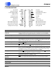
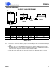
Table Of Contents
- Features
- 1. Characteristics & Specifications
- 2. Overview
- 3. Functional Description
- 3.1 Pulse-Rate Output
- 3.2 Pulse Output for Normal Format, Stepper Motor Format and Mechanical Counter Format
- 3.3 Auto-boot Mode Using EEPROM
- 3.4 Interrupt and Watchdog Timer
- 3.5 Oscillator Characteristics
- 3.6 Analog Inputs
- 3.7 Voltage Reference
- 3.8 Calibration
- 3.9 Phase Compensation
- 3.10 Time-Base Calibration Register
- 3.11 Power Offset Register
- 3.12 Input Protection - Current Limit
- 3.13 Input Filtering
- 3.14 Protection Against High-voltage and/or High-current Surges
- 3.15 Improving RFI Immunity
- 3.16 PCB Layout
- 4. Serial Port Overview
- 5. Register Descriptions
- 6. Pin Descriptions
- 7. Package Dimensions
- 8. Ordering Information
- 9. Environmental, Manufacturing, & Handling Information
- 10. Revision History
CS5460A
52 DS487F5
Voltage
Reference Output
11 VREFOUT - The on-chip voltage reference is output from this pin. The voltage reference
has a nominal magnitude of 2.5 V and is reference to the VA- pin on the converter.
Voltage
Reference Input
12 VREFIN - The voltage input to this pin establishes the voltage reference for the on-chip
modulator.
Differential
Current Inputs
15,16 IIN+, IIN- - Differential analog input pins for current channel.
Power Supply Connections
Positive
Digital Supply
3 VD+ - The positive digital supply is nominally +5 V ±10% relative to DGND.
Digital Ground
4 DGND - The common-mode potential of digital ground must be equal to or above the
common-mode potential of VA-.
Negative
Analog Supply
13 VA- - The negative analog supply pin must be at the lowest potential.
Positive
Analog Supply
14 VA+ - The positive analog supply is nominally +5 V ±10% relative to VA-.
Power Fail Monitor
17 PFMON - The power fail Monitor pin monitors the analog supply. Typical threshold level
(PMLO) is 2.45 V with respect to the VA- pin. If PFMON voltage threshold is tripped, the
LSD (low-supply detect) bit is set in the Status Register. Once the LSD bit has been set,
it will not be able to be reset until the PFMON voltage increases ~100 mV (typical) above
the PMLO voltage. Therefore, there is hysteresis in the PFMON function.
RESET 19
Reset - When reset is taken low, all internal registers are set to their default states.
Other
No Connection 18 NC - No connection. Pin should be left floating.