
Manual
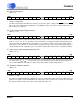
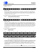
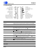
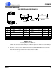
Table Of Contents
- Features
- 1. Characteristics & Specifications
- 2. Overview
- 3. Functional Description
- 3.1 Pulse-Rate Output
- 3.2 Pulse Output for Normal Format, Stepper Motor Format and Mechanical Counter Format
- 3.3 Auto-boot Mode Using EEPROM
- 3.4 Interrupt and Watchdog Timer
- 3.5 Oscillator Characteristics
- 3.6 Analog Inputs
- 3.7 Voltage Reference
- 3.8 Calibration
- 3.9 Phase Compensation
- 3.10 Time-Base Calibration Register
- 3.11 Power Offset Register
- 3.12 Input Protection - Current Limit
- 3.13 Input Filtering
- 3.14 Protection Against High-voltage and/or High-current Surges
- 3.15 Improving RFI Immunity
- 3.16 PCB Layout
- 4. Serial Port Overview
- 5. Register Descriptions
- 6. Pin Descriptions
- 7. Package Dimensions
- 8. Ordering Information
- 9. Environmental, Manufacturing, & Handling Information
- 10. Revision History

CS5460A
DS487F5 51
6. PIN DESCRIPTIONS
1
2
3
4
5
6
7
817
18
19
20
21
22
23
24
9
10
11
12 13
14
15
16
Crystal Out XOUT
CPU Clock Output CPUCLK
Positive Digital Supply VD+
Digital Ground DGND
Serial Clock Input SCLK
Serial Data Output SDO
Chip Select CS
Mode Select MODE
Differential Voltage Input VIN+
Differential Voltage Input VIN-
Voltage Reference Output VREFOUT
Voltage Reference Input VREFIN
XIN Crystal In
SDI Serial Data Input
EDIR
Energy Direction Indicator
EOUT
Energy Output
INT
Interrupt
RESET
Reset
NC No Connect
PFMON Power Fail Monitor
IIN+ Differential Current Input
IIN- Differential Current Input
VA+ Positive Analog Supply
VA- Analog Ground
Clock Generator
Crystal Out
Crystal In
1,24 XOUT, XIN - A gate inside the chip is connected to these pins and can be used with a
crystal to provide the system clock for the device. Alternatively, an external (CMOS
compatible clock) can be supplied into XIN pin to provide the system clock for the device.
CPU Clock Output
2 CPUCLK - Output of on-chip oscillator which can drive one standard CMOS load.
Control Pins and Serial Data I/O
Serial Clock Input
5 SCLK - A clock signal on this pin determines the input and output rate of the data for the
SDI and SDO pins respectively. This input is a Schmitt trigger to allow for slow rise time
signals. The SCLK pin will recognize clocks only when CS is low.
Serial Data Output
6 SDO - SDO is the output pin of the serial data port. Its output will be in a high impedance
state when CS is high.
Chip Select
7 CS - When low, the port will recognize SCLK. An active high on this pin forces the SDO
pin to a high impedance state. CS
should be changed when SCLK is low.
Mode Select
8 MODE - When at logic high, the CS5460A can perform the auto-boot sequence with the
aid of an external serial EEPROM to receive commands and settings. When at logic low,
the CS5460A assumes normal “host mode” operation. This pin is pulled down to logic
low if left unconnected, by an internal pull-down resistor to DGND.
Interrupt
20 INT - When INT goes low it signals that an enabled event has occurred. INT is cleared
(logic 1) by writing the appropriate command to the CS5460A.
Energy Output
21 EOUT - The energy output pin output a fixed-width pulse rate output with a rate (pro-
grammable) proportional to real (billable) energy.
Energy Direction
Indicator
22
EDIR
- The energy direction indicator indicates if the measured energy is negative.
Serial Data Input
23 SDI - the input pin of the serial data port. Data will be input at a rate determined by SCLK.
Measurement and Reference Input
Differential
Voltage Inputs
9,10 VIN+, VIN- - Differential analog input pins for voltage channel.