
Manual
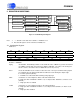
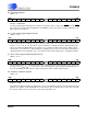
Table Of Contents
- Features
- 1. Characteristics & Specifications
- 2. Overview
- 3. Functional Description
- 3.1 Pulse-Rate Output
- 3.2 Pulse Output for Normal Format, Stepper Motor Format and Mechanical Counter Format
- 3.3 Auto-boot Mode Using EEPROM
- 3.4 Interrupt and Watchdog Timer
- 3.5 Oscillator Characteristics
- 3.6 Analog Inputs
- 3.7 Voltage Reference
- 3.8 Calibration
- 3.9 Phase Compensation
- 3.10 Time-Base Calibration Register
- 3.11 Power Offset Register
- 3.12 Input Protection - Current Limit
- 3.13 Input Filtering
- 3.14 Protection Against High-voltage and/or High-current Surges
- 3.15 Improving RFI Immunity
- 3.16 PCB Layout
- 4. Serial Port Overview
- 5. Register Descriptions
- 6. Pin Descriptions
- 7. Package Dimensions
- 8. Ordering Information
- 9. Environmental, Manufacturing, & Handling Information
- 10. Revision History
CS5460A
50 DS487F5
CRDY Conversion Ready. Indicates a new conversion is ready. This will occur at the output word rate,
which is usually 4 kHz.
EDIR Set whenever the EOUT bit asserted (see below) if the accumulated energy is negative.
EOUT Indicates that enough positive/negative energy has been reached within the internal EOUT
En-
ergy Accumulation Register (not accessible to user) to mandate the generation of one or more
pulses on the EOUT
pin (if enabled, see Configuration Register). The energy flow may indicate
negative energy or positive energy. (The sign is determined by the EDIR bit, described above).
This EOUT bit is cleared automatically when the energy rate drops below the level that produc-
es a 4 kHz EOUT pin rate. The bit can also be cleared by writing to the Status Register. This
status bit is set with a maximum frequency of 4 kHz (when MCLK/K is 4.096 MHz). When
MCLK/K is not equal to 4.096 MHz, the user should scale the pulse-rate by a factor of
4.096 MHz / (MCLK/K) to get the actual pulse-rate.
DRDY Data Ready. When running in ’single computation cycle’ or ’continuous computation cycles’
data acquisition modes, this bit will indicate the end of computation cycles. When running cali-
brations, this bit indicates that the calibration sequence has completed, and the results have
been stored in the offset or gain registers.
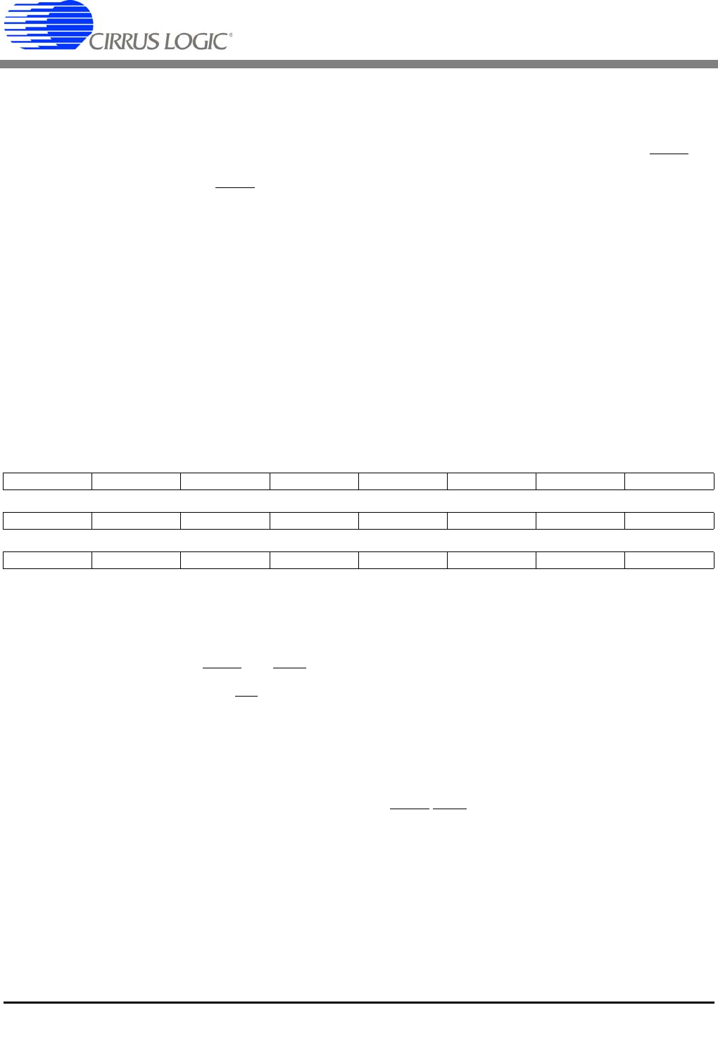
5.12 Control Register
Address: 28
Default** = 0x000000
STOP 1 = used to terminate the new EEBOOT sequence.
Res Reserved. These bits must be set to zero.
MECH 1 = widens EOUT
and EDIR pulses for mechanical counters.
INTL 1 = converts the INT
output to open drain configuration.
SYNC 1 = forces internal A/D converter clock to synchronize to the initiation of a conversion command.
NOCPU 1 = converts the CPUCLK output to a one-bit output port. Reduces power consumption.
NOOSC 1 = saves power by disabling the crystal oscillator for external drive.
STEP 1 = enables stepper-motor signals on the EOUT
/EDIR pins.
23 22 21 20 19 18 17 16
ResResResResResResResRes
15 14 13 12 11 10 9 8
Res Res Res Res Res Res Res STOP
76543210
Res MECH Res INTL SYNC NOCPU NOOSC STEP