
Manual
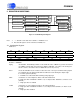
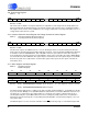
Table Of Contents
- Features
- 1. Characteristics & Specifications
- 2. Overview
- 3. Functional Description
- 3.1 Pulse-Rate Output
- 3.2 Pulse Output for Normal Format, Stepper Motor Format and Mechanical Counter Format
- 3.3 Auto-boot Mode Using EEPROM
- 3.4 Interrupt and Watchdog Timer
- 3.5 Oscillator Characteristics
- 3.6 Analog Inputs
- 3.7 Voltage Reference
- 3.8 Calibration
- 3.9 Phase Compensation
- 3.10 Time-Base Calibration Register
- 3.11 Power Offset Register
- 3.12 Input Protection - Current Limit
- 3.13 Input Filtering
- 3.14 Protection Against High-voltage and/or High-current Surges
- 3.15 Improving RFI Immunity
- 3.16 PCB Layout
- 4. Serial Port Overview
- 5. Register Descriptions
- 6. Pin Descriptions
- 7. Package Dimensions
- 8. Ordering Information
- 9. Environmental, Manufacturing, & Handling Information
- 10. Revision History
CS5460A
48 DS487F5
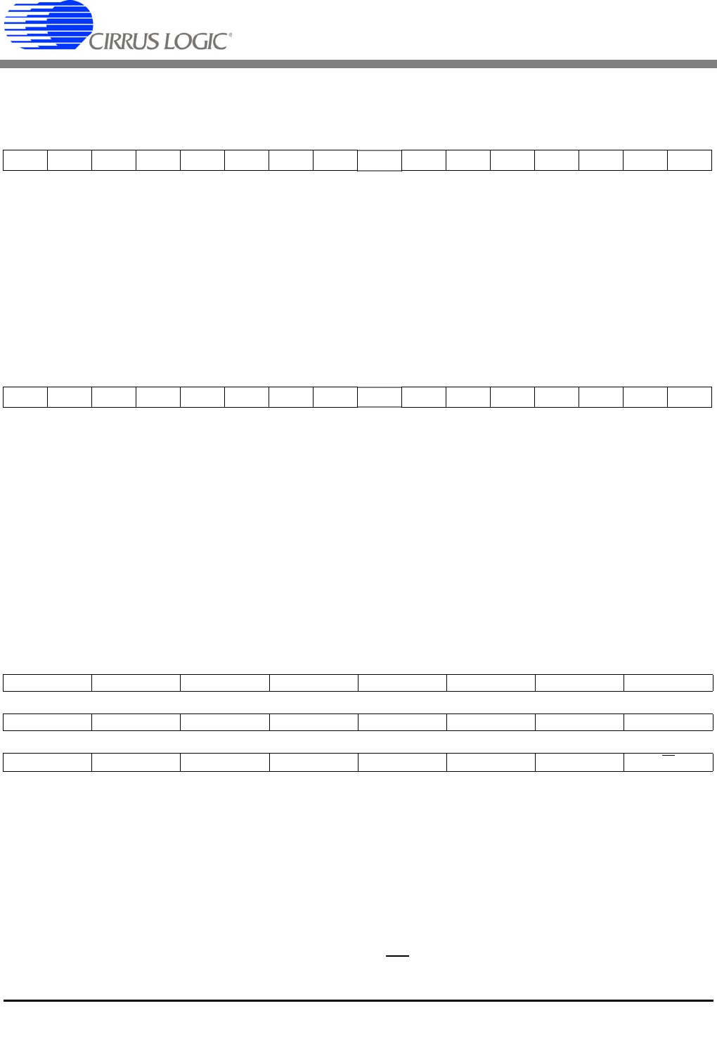
5.9 Power Offset Register
Address: 14
Default** = 0.000
This offset value is added to each power value that is computed for each voltage/current sample pair before
being accumulated in the Energy Register. The numeric format of this register is two’s complement notation.
This register can be used to offset contributions to the energy result that are caused by undesirable sources of
energy that are inherent in the system.
5.10 Current Channel AC Offset Register and Voltage Channel AC Offset Register
Address: 16 (Current Channel AC Offset Register)
17 (Voltage Channel AC Offset Register)
Default** = 0.000
The AC offset registers are initialized to zero on reset, allowing the device to function and perform measure-
ments. First, the ground-level input should be applied to the inputs. Then the AC Offset Calibration Command
is should be sent to the CS5460A. After ~(6N + 30) A/D conversion cycles (where N is the value of the Cy-
cle-Count Register), the gain register(s) is loaded with the square of the system AC offset value. DRDY will be
asserted at the end of the calibration. The register may be read and stored so the register may be restored with
the desired system offset compensation. Note that this register value represents the square of the AC cur-
rent/voltage offset.
5.11 Status Register and Mask Register
Address: 15 (Status Register)
26 (Mask Register)
Default** = Binary: 00000000000000xxxx000001 (Status Register) {x = state depends on device revision}
Binary: 000000000000000000000000 (Mask Register)
The Status Register indicates the condition of the chip. In normal operation writing a '1' to a bit will cause the bit
to go to the '0' state. Writing a '0' to a bit will maintain the status bit in its current state. With this feature the user
can write logic ‘1’ values back to the Status Register to selectively clear only those bits that have been re-
solved/registered by the system MCU, without concern of clearing any newly set bits. Even if a status bit is
masked to prevent the interrupt, the corresponding status bit will still be set in the Status Register so the user
can poll the status.
The Mask Register is used to control the activation of the INT
pin. Placing a logic '1' in the Mask Register will
MSB LSB
-(2
0
)2
-1
2
-2
2
-3
2
-4
2
-5
2
-6
2
-7
.....
2
-17
2
-18
2
-19
2
-20
2
-21
2
-22
2
-23
MSB LSB
2
-13
2
-14
2
-15
2
-16
2
-17
2
-18
2
-19
2
-20
.....
2
-30
2
-31
2
-32
2
-33
2
-34
2
-35
2
-36
23 22 21 20 19 18 17 16
DRDY EOUT EDIR CRDY MATH Res IOR VOR
15 14 13 12 11 10 9 8
PWOR IROR VROR EOR EOOR Res ID3 ID2
76543210
ID1 ID0 WDT VOD IOD LSD 0
IC