
Manual
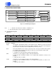
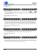
Table Of Contents
- Features
- 1. Characteristics & Specifications
- 2. Overview
- 3. Functional Description
- 3.1 Pulse-Rate Output
- 3.2 Pulse Output for Normal Format, Stepper Motor Format and Mechanical Counter Format
- 3.3 Auto-boot Mode Using EEPROM
- 3.4 Interrupt and Watchdog Timer
- 3.5 Oscillator Characteristics
- 3.6 Analog Inputs
- 3.7 Voltage Reference
- 3.8 Calibration
- 3.9 Phase Compensation
- 3.10 Time-Base Calibration Register
- 3.11 Power Offset Register
- 3.12 Input Protection - Current Limit
- 3.13 Input Filtering
- 3.14 Protection Against High-voltage and/or High-current Surges
- 3.15 Improving RFI Immunity
- 3.16 PCB Layout
- 4. Serial Port Overview
- 5. Register Descriptions
- 6. Pin Descriptions
- 7. Package Dimensions
- 8. Ordering Information
- 9. Environmental, Manufacturing, & Handling Information
- 10. Revision History
CS5460A
44 DS487F5
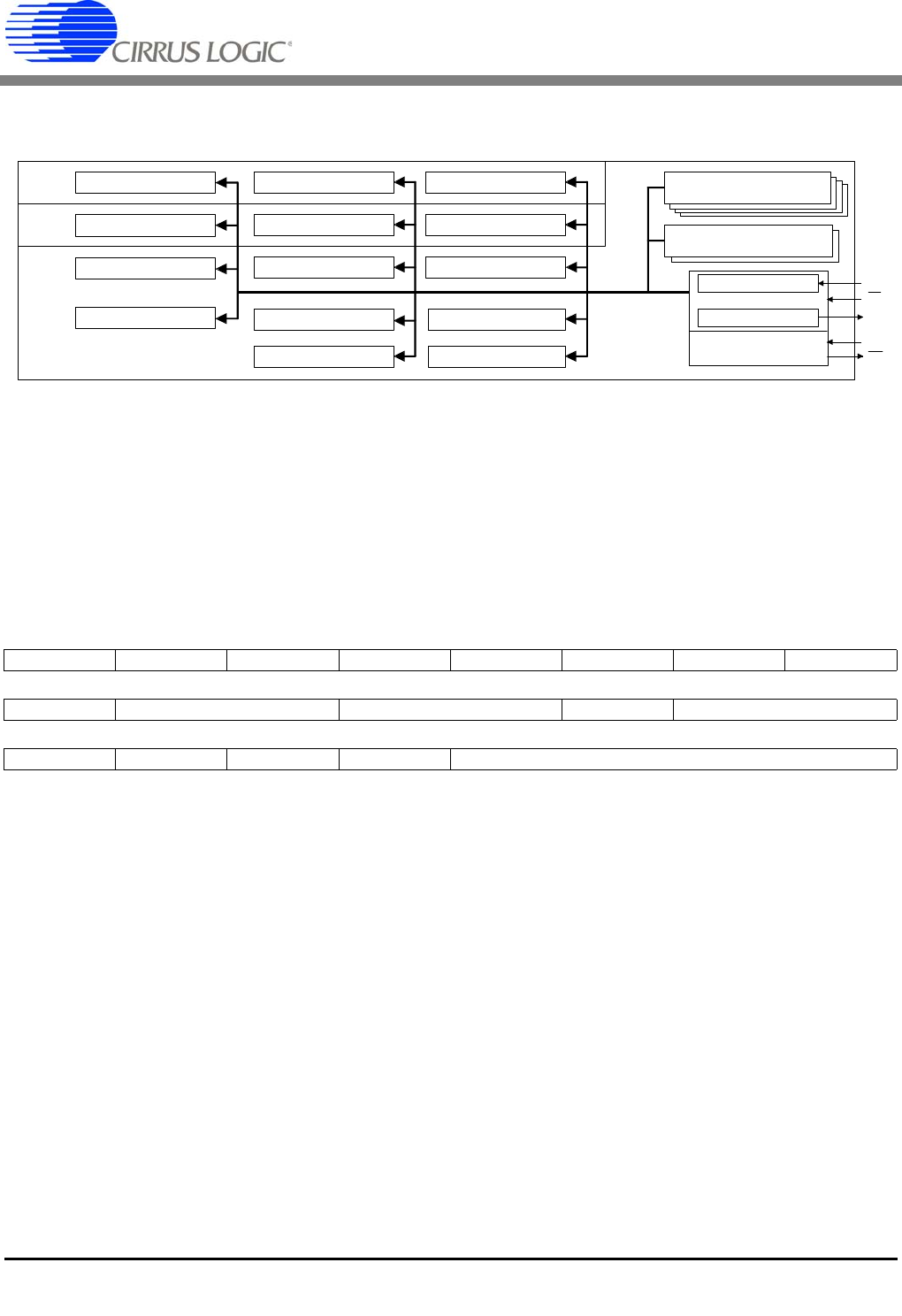
5. REGISTER DESCRIPTIONS
Note: 1. ** “default” => bit status after software or hardware reset
2. Note that all registers can be read from, and written to.
5.1 Configuration Register
Address: 0
Default** = 0x000001
K[3:0] Clock divider. A 4 bit binary number used to divide the value of MCLK to generate the internal
clock DCLK. The internal clock frequency is DCLK = MCLK/K. The value of K can range be-
tween 1 and 16. Note that a value of “0000” will set K to 16 (not zero).
iCPU Inverts the CPUCLK clock. In order to reduce the level of noise present when analog signals
are sampled, the logic driven by CPUCLK should not be active during the sample edge.
0 = normal operation (default)
1 = minimize noise when CPUCLK is driving rising edge logic
IHPF Control the use of the High Pass Filter on the Current Channel.
0 = High-pass filter is disabled. If VHPF is set, use all-pass filter. Otherwise, no filter is used.
(default)
1 = High-pass filter is enabled.
VHPF Control the use of the High Pass Filter on the voltage Channel.
0 = High-pass filter is disabled. If IHPF is set, use all-pass filter. Otherwise, no filter is used.
(default)
1 = High-pass filter enabled
23 22 21 20 19 18 17 16
PC6 PC5 PC4 PC3 PC2 PC1 PC0 Gi
15 14 13 12 11 10 9 8
EWA Res Res SI1 SI0 EOD DL1 DL0
76543210
RS VHPF IHPF iCPU K3 K2 K1 K0
Current
Channel
Voltage
Channel
Cycle-Counter Registe
Status Register (1 × 24)
Serial Interface
Mask Register (1 × 24)
Unsigned Output Registers (2 × 24)
(I , V )
Command Word
State Machine
Transmit Buffer
Receive Buffer
Signed Output Registers (4 × 24)
(I, V, P, E)
RMS RMS
24-Bit
SDI
CS
SDO
SCLK
INT
AC Offset Register (1 x 24)
AC Offset Register (1 x 24)
Control Register (1 x 24)
Power Offset Register (1 x 24)
Configuration Register (1 × 24)
Pulse-Rate Register (1 × 24)
Offset Register (1 × 24)DC
Offset Register (1 × 24)DC Gain Register (1 × 24)AC/DC
Gain Register (1 × 24)AC/DC
r(1×24)
Timebase Cal. Register (1 x 24)
Figure 21. CS5460A Register Diagram