
Manual
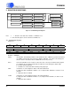
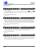
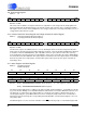
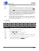
Table Of Contents
- Features
- 1. Characteristics & Specifications
- 2. Overview
- 3. Functional Description
- 3.1 Pulse-Rate Output
- 3.2 Pulse Output for Normal Format, Stepper Motor Format and Mechanical Counter Format
- 3.3 Auto-boot Mode Using EEPROM
- 3.4 Interrupt and Watchdog Timer
- 3.5 Oscillator Characteristics
- 3.6 Analog Inputs
- 3.7 Voltage Reference
- 3.8 Calibration
- 3.9 Phase Compensation
- 3.10 Time-Base Calibration Register
- 3.11 Power Offset Register
- 3.12 Input Protection - Current Limit
- 3.13 Input Filtering
- 3.14 Protection Against High-voltage and/or High-current Surges
- 3.15 Improving RFI Immunity
- 3.16 PCB Layout
- 4. Serial Port Overview
- 5. Register Descriptions
- 6. Pin Descriptions
- 7. Package Dimensions
- 8. Ordering Information
- 9. Environmental, Manufacturing, & Handling Information
- 10. Revision History

CS5460A
DS487F5 41
4.1.7 Register Read/Write
This command informs the state machine that a register access is required. On reads the addressed register is load-
ed into the output buffer and clocked out by SCLK. On writes the data is clocked into the input buffer and transferred
to the addressed register on the 24
th
SCLK.
W/R
Write/Read control
0 = Read register
1 = Write register
RA[4:0] Register address bits. Binary encoded 0 to 31. All registers are 24 bits in length.
Address Abbreviation Name/Description
00000 Config Configuration Register.
00001 I
DCoff Current Channel DC Offset Register.
00010 I
gn Current Channel Gain Register.
00011 V
DCoff Voltage Channel DC Offset Register.
00100 V
gn Voltage Channel Gain Register.
00101 Cycle Count Number of A/D cycles per computation cycle.
00110 Pulse-Rate Used to set the energy-to-pulse ratio on EOUT
(and EDIR).
00111 I Instantaneous Current Register (most recent current sample).
01000 V Instantaneous Voltage Register (most recent voltage sample).
01001 P Instantaneous Power Register (most recent power sample).
01010 E Energy Register (accumulated over latest computation cycle).
01011 I
RMS
RMS Current Register (computed over latest computation cycle).
01100 V
RMS
RMS Voltage Register (computed over latest computation cycle).
01101 TBC Timebase Calibration Register.
01110 Poff Power Offset Register.
01111 Status Status Register.
10000 I
ACoff Current Channel AC Offset Register.
10001 V
ACoff Voltage Channel AC Offset Register.
10010 Res Reserved †
. . .
. . .
10111 Res Reserved †
11000 Res Reserved †
11001 Test Reserved †
11010 Mask Mask Register.
11011 Res Reserved †
11100 Ctrl Control Register.
11101 Res Reserved †
. . .
. . .
11111 Res Reserved †
† These registers are for Internal Use only and should not be written to.
B7 B6 B5 B4 B3 B2 B1 B0
0W/R
RA4 RA3 RA2 RA1 RA0 0