
Manual
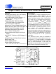
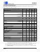
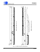
Table Of Contents
- Features
- 1. Characteristics & Specifications
- 2. Overview
- 3. Functional Description
- 3.1 Pulse-Rate Output
- 3.2 Pulse Output for Normal Format, Stepper Motor Format and Mechanical Counter Format
- 3.3 Auto-boot Mode Using EEPROM
- 3.4 Interrupt and Watchdog Timer
- 3.5 Oscillator Characteristics
- 3.6 Analog Inputs
- 3.7 Voltage Reference
- 3.8 Calibration
- 3.9 Phase Compensation
- 3.10 Time-Base Calibration Register
- 3.11 Power Offset Register
- 3.12 Input Protection - Current Limit
- 3.13 Input Filtering
- 3.14 Protection Against High-voltage and/or High-current Surges
- 3.15 Improving RFI Immunity
- 3.16 PCB Layout
- 4. Serial Port Overview
- 5. Register Descriptions
- 6. Pin Descriptions
- 7. Package Dimensions
- 8. Ordering Information
- 9. Environmental, Manufacturing, & Handling Information
- 10. Revision History

CS5460A
DS487F5 3
3.8.7.4 DC Gain Calibration Sequence ......................................................... 31
3.8.8 Duration of Calibration Sequence ....................................................................... 31
3.9 Phase Compensation ...................................................................................................... 31
3.10 Time-Base Calibration Register ..................................................................................... 32
3.11 Power Offset Register ................................................................................................... 32
3.12 Input Protection - Current Limit ...................................................................................... 32
3.13 Input Filtering ................................................................................................................. 34
3.14 Protection Against High-voltage and/or High-current Surges ........................................ 37
3.15 Improving RFI Immunity ................................................................................................ 38
3.16 PCB Layout ................................................................................................................... 38
4. SERIAL PORT OVERVIEW .................................................................................................... 38
4.1 Commands (Write Only) .................................................................................................. 39
4.2 Serial Port Interface ......................................................................................................... 42
4.3 Serial Read and Write ..................................................................................................... 42
4.3.1 Register Write ..................................................................................................... 42
4.3.2 Register Read ..................................................................................................... 42
4.4 System Initialization ......................................................................................................... 42
4.5 Serial Port Initialization .................................................................................................... 43
4.6 CS5460A Power States ................................................................................................... 43
5. REGISTER DESCRIPTIONS ................................................................................................. 44
5.1 Configuration Register......................................................................................................44
5.2 Current Channel DC Offset Register and Voltage Channel DC Offset Register .............. 46
5.3 Current Channel Gain Register and Voltage Channel Gain Register............................... 46
5.4 Cycle Count Register........................................................................................................46
5.5 Pulse-Rate Register .........................................................................................................47
5.6 I,V,P,E Signed Output Register Results ........................................................................... 47
5.7 IRMS, VRMS Unsigned Output Register Results............................................................. 47
5.8 Timebase Calibration Register ......................................................................................... 47
5.9 Power Offset Register ...................................................................................................... 48
5.10 Current Channel AC Offset Register and Voltage Channel AC Offset Register............. 48
5.11 Status Register and Mask Register ................................................................................ 48
5.12 Control Register.............................................................................................................. 50
6. PIN DESCRIPTIONS .............................................................................................................. 51
7. PACKAGE DIMENSIONS ...................................................................................................... 53
8. ORDERING INFORMATION ................................................................................................. 54
9. ENVIRONMENTAL, MANUFACTURING, & HANDLING INFORMATION ............................ 54
10. REVISION HISTORY ............................................................................................................. 54