
Manual
Table Of Contents
- Features
- 1. Characteristics & Specifications
- 2. Overview
- 3. Functional Description
- 3.1 Pulse-Rate Output
- 3.2 Pulse Output for Normal Format, Stepper Motor Format and Mechanical Counter Format
- 3.3 Auto-boot Mode Using EEPROM
- 3.4 Interrupt and Watchdog Timer
- 3.5 Oscillator Characteristics
- 3.6 Analog Inputs
- 3.7 Voltage Reference
- 3.8 Calibration
- 3.9 Phase Compensation
- 3.10 Time-Base Calibration Register
- 3.11 Power Offset Register
- 3.12 Input Protection - Current Limit
- 3.13 Input Filtering
- 3.14 Protection Against High-voltage and/or High-current Surges
- 3.15 Improving RFI Immunity
- 3.16 PCB Layout
- 4. Serial Port Overview
- 5. Register Descriptions
- 6. Pin Descriptions
- 7. Package Dimensions
- 8. Ordering Information
- 9. Environmental, Manufacturing, & Handling Information
- 10. Revision History
CS5460A
10 DS487F5
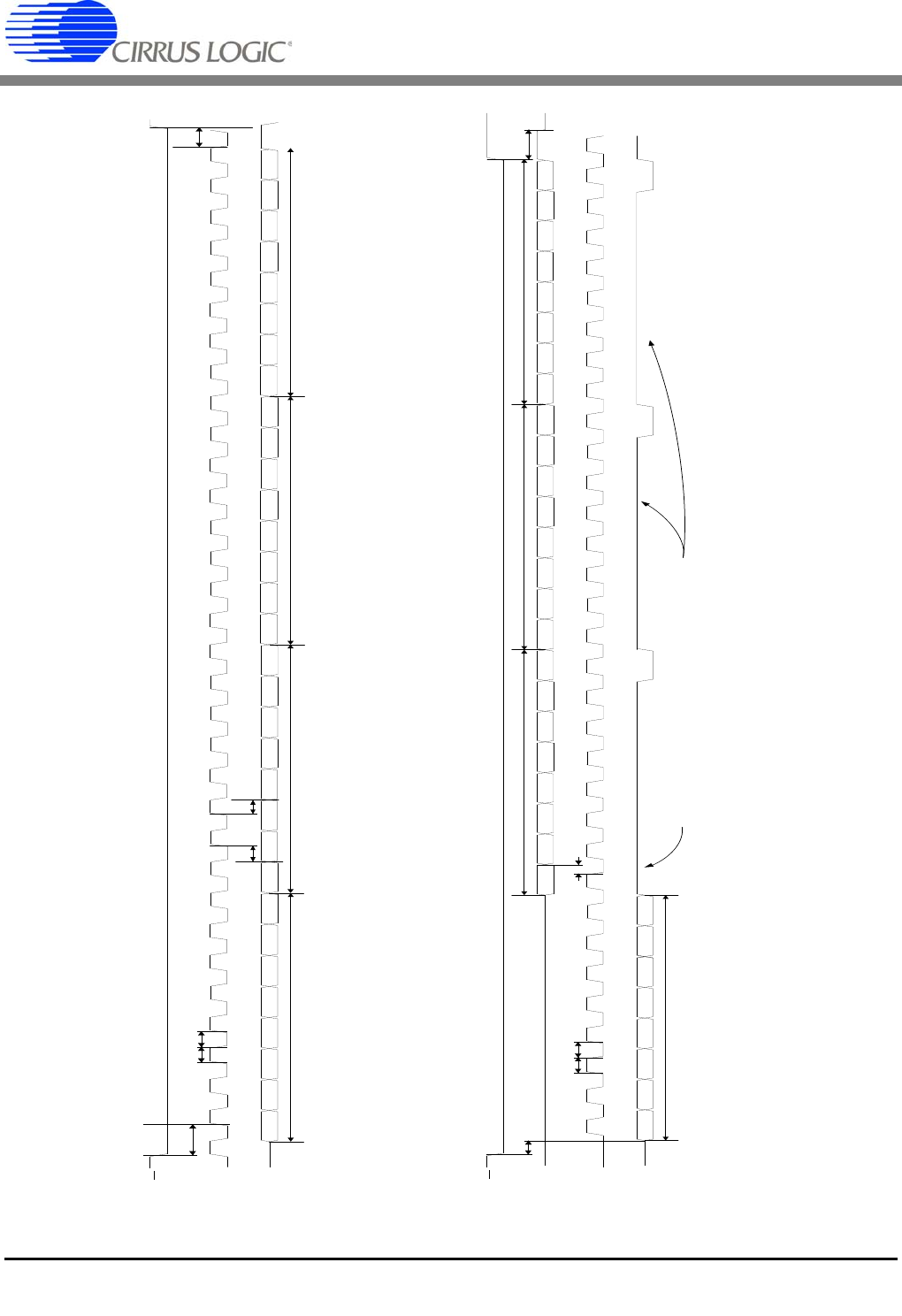
CS
SCLK
MSB MSB - 1
LSB
t
2
t
1
t
3
SDI
MSB MSB - 1
LSB
Command Time 8 SCLKs
LSB
t
6
MSB MSB - 1
LSB
MSB MSB - 1
High Byte Mid Byte Low Byte
t
t
45
SDI Write Timing (Not to Scale)
CS
SDO
SCLK
MSB MSB - 1
LSB
t
2
t
1
t
8
t
7
SDI
MSB MSB - 1
LSB
Command Time 8 SCLKs
LSB
t
9
MSB MSB - 1
LSB
MSB MSB - 1
High Byte Mid Byte
Low Byte
M
u
s
t
s
t
r
o
b
e
"
S
Y
N
C
0
"
c
o
m
m
a
n
d
o
n
S
D
I
w
h
e
n
r
e
a
d
i
n
g
e
a
c
h
b
y
t
e
o
f
d
a
t
a
f
r
o
m
S
D
O
.
SDO Read Timing (Not to Scale)
Figure 1. CS5460A Read and Write Timing Diagrams