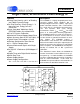
CS5460A Single Phase, Bi-directional Power/Energy IC Features Description Energy The CS5460A is a highly integrated power measurement solution which combines two Analog-to-digital Converters (ADCs), high-speed power calculation functions, and a serial interface on a single chip. It is designed to accurately measure and calculate: Real (True) Energy, Instantaneous Power, IRMS, and VRMS for single phase 2- or 3-wire power metering applications.
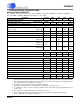
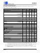
CS5460A TABLE OF CONTENTS 1. CHARACTERISTICS & SPECIFICATIONS ............................................................................. 5 ANALOG CHARACTERISTICS ................................................................................................ 5 VREFOUT REFERENCE OUTPUT VOLTAGE........................................................................ 7 5V DIGITAL CHARACTERISTICS............................................................................................ 7 3.
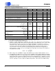
CS5460A 3.8.7.4 DC Gain Calibration Sequence ......................................................... 31 3.8.8 Duration of Calibration Sequence ....................................................................... 31 3.9 Phase Compensation ...................................................................................................... 31 3.10 Time-Base Calibration Register ..................................................................................... 32 3.11 Power Offset Register ...........
CS5460A LIST OF FIGURES Figure 1. CS5460A Read and Write Timing Diagrams.................................................................. 10 Figure 2. CS5460A Auto-Boot Sequence Timing.......................................................................... 11 Figure 3. Data Flow. ...................................................................................................................... 13 Figure 4. Voltage Input Filter Characteristics ...........................................................
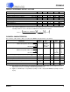
CS5460A 1. CHARACTERISTICS & SPECIFICATIONS ANALOG CHARACTERISTICS (TA = -40 °C to +85 °C; VA+ = VD+ = +5 V ±10%; VREFIN = +2.5 V; VA- = AGND = 0 V; MCLK = 4.096 MHz, K = 1; N = 4000 ==> OWR = 4000 Sps.)(See Notes 1, 2, 3, 4, and 5.) Parameter Symbol Min Typ Max Unit CMRR 80 - - dB - 5 - nV/°C IIN - - 500 100 mVP-P mVP-P THDI 80 - - dB -0.
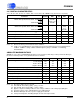
CS5460A ANALOG CHARACTERISTICS (Continued) Parameter Symbol Min Typ Max Unit -2.4 - +2.5 ° - DCLK/1024 - Sps - DCLK/8 - Sps 25 - 100 %F.S. Dynamic Characteristics Phase Compensation Range (Voltage Channel, 60 Hz) High Rate Filter Output Word Rate Input Sample Rate (Both Channels) OWR DCLK = MCLK/K Full Scale DC Calibration Range (Note 7) FSCR Channel-to-Channel Time-Shift Error (when PC[6:0] bits are set to “0000000”) 1.0 High Pass Filter Pole Frequency -3 dB µs - 0.
CS5460A VREFOUT REFERENCE OUTPUT VOLTAGE Parameter Reference Output Output Voltage VREFOUT Temperature Coefficient (Note 12) Load Regulation (Output Current 1 µA Source or Sink) Reference Input Input Voltage Range Input Capacitance Input CVF Current Symbol Min Typ Max Unit REFOUT TVREFOUT VR +2.4 - 30 6 +2.6 60 10 V ppm/°C mV VREFIN +2.4 - +2.5 4 25 +2.6 - V pF nA Notes: 12. The voltage at VREFOUT is measured across the temperature range.
CS5460A 3.3 V DIGITAL CHARACTERISTICS (TA = -40 °C to +85 °C; VA+ = 5 V ±10%, VD+ = 3.3 V ±10%; VA-, DGND = 0 V) (See Notes 3, 4, and 13) Parameter Symbol Min Typ Max Unit High-Level Input Voltage All Pins Except XIN, XOUT, SCLK, and RESET XIN SCLK and RESET VIH 0.6 VD+ (VD+) - 0.5 0.8VD+ - - V V V Low-Level Input Voltage All Pins Except XIN, XOUT, SCLK, and RESET XIN SCLK and RESET VIL - - 0.48 0.3 0.2VD+ V V V High-Level Output Voltage (except XIN, XOUT) Iout = +5 mA VOH (VD+) - 1.
CS5460A SWITCHING CHARACTERISTICS (TA = -40 °C to +85 °C; VA+ = 5.0 V ±10%; VD+ = 3.0 V ±10% or 5.0 V ±10%; VA- = 0.0 V; Logic Levels: Logic 0 = 0.0 V, Logic 1 = VD+; CL = 50 pF)) Parameter Master Clock FrequencyCrystal/Internal Gate Oscillator (Note 24) Master Clock Duty Cycle CPUCLK Duty Cycle (Note 25) Rise Times Any Digital Input Except SCLK (Note 26) SCLK Any Digital Output Fall Times Any Digital Input Except SCLK (Note 26) SCLK Any Digital Output Start-up Oscillator Start-Up Time XTAL = 4.
SDI SCLK SDO CS SDI SCLK CS t 7 t3 MSB MSB MSB - 1 MSB - 1 t2 t2 Command Time 8 SCLKs t1 Command Time 8 SCLKs t1 LSB LSB MSB t MSB 8 4 MSB - 1 MSB - 1 t 5 MSB MSB - 1 High Byte LSB MSB MSB - 1 Mid Byte SDO Read Timing (Not to Scale) Mid Byte SDI Write Timing (Not to Scale) High Byte LSB Must strobe "SYNC0" command on SDI when reading each byte of data from SDO. t LSB LSB MSB MSB MSB - 1 MSB - 1 Low Byte Low Byte LSB LSB t9 t 6 CS5460A Figure 1.
DS487F5 (Input) SDI (Output) SDO (Output) SCLK (Output) CS (Input) RES (Input) MODE t 12 t 13 t 14 1 t1 t 10 Figure 2.
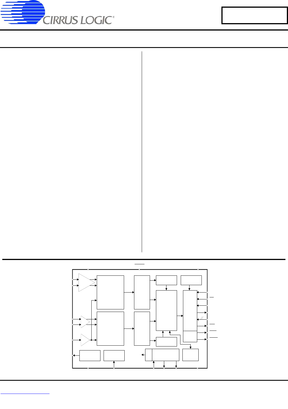
CS5460A 2. OVERVIEW 2.1.1 Modulators The CS5460A is a CMOS monolithic power measurement device with a real power/energy computation engine. The CS5460A combines two programmable gain amplifiers, two modulators, two high rate filters, system calibration, and rms/power calculation functions to provide instantaneous voltage/current/power data samples as well as periodic computation results for real (billable) energy, VRMS, and IRMS.
CS5460A V* VDCoff* V gn * VOLTAGE DELAY REG SINC 2 DELAY REG FIR + HPF x VACoff* x APF - SINC 2 Poff* Configuration Register * PC[6:0] Bits N V RMS * TBC * N x ÷N + P* 4096 x E* E out E to F E dir PULSE-RATE* CURRENT SINC 4 FIR + HPF x IDCoff* I gn * APF x I* - SINC 2 N ÷N I RMS * IACoff* * DENOTES REGISTER NAME Figure 3. Data Flow.
CS5460A full-scale. Note that the 24-bit signed output words are expressed in two’s complement format. The 24-bit data words in the CS5460A output registers represent values between 0 and 1 (for unsigned output registers) or between -1 and +1 (for signed output registers). A register value of 1 represents the maximum possible value. Note that a value of 1.0 is never actually obtained in the registers of the CS5460A.
CS5460A a 4.096 MHz clock at XIN, and K = 1, instantaneous A/D conversions for voltage, current, and power are performed at a 4000 Sps rate, whereas IRMS, VRMS, and energy calculations are performed at a 1 Sps rate. 2.2.1 CS5460A Linearity Performance Table 2 lists the range of input levels (as a percentage of full-scale) over which the (linearity + variation) of the results in the Vrms, Irms and Energy Registers are guaranteed to be within ±0.
CS5460A result from one of several result registers. The first 8 SCLKs are used to clock in the command to determine which register is to be read. The last 24 SCLKs are used to read the desired register. After reading the data, the serial port remains in the active state, and waits for a new command to be issued. (See Section 3 for more details on reading register data from the CS5460A). 2.2.
CS5460A complete isolation from the power lines. This isolation is achieved using three transformers. One transformer is a general-purpose voltage transformer, used to supply the on-board DC power to the CS5460A. A second transformer is a high-precision, low-impedance voltage transformer (often called a ‘potential transformer’) with very little roll-off/phase delay, even at the higher harmonics. A current transformer is then used to sense the line current.
CS5460A N 10 k 5 k 120 VAC L Voltage Transformer 200 12 VAC 10 200 0.1 µF 0.1µF + 14 VA+ 200µF 12 VAC 3 VD+ CS5460A R *V+ M:1 1k 9 C*V+* 1k * C *Vdiff C*V-* Low Phase-Shift Potential Transformer 10 VIN- 17 PFMON 2 CPUCLK 1 XOUT XIN 24 R *VR*I- N:1 15 C *I+* 1k RBurden 1k Current Transformer VIN+ C*I- * R*I+ * C *Idiff 16 12 11 IIN- RESET NOTE: Current channel input measures voltage (just like voltage input). IIN+ VREFIN VREFOUT 0.
CS5460A 240 VAC 120 VAC L1 5 k 10 k 120 VAC N L2 500 500 10 0.1 µF + 470 nF 100 µF Earth Ground 0.1 µF 14 VA+ 3 VD+ CS5460A 9 VIN+ C ** V+ R3 R2 * C*Vdiff R4 ** CV- R1 10 VIN16 IIN+ 1k * R I+ * C*Idiff C ** I- 1k XIN 24 2.5 MHz to 20 MHz Optional Clock Source C ** I+ RBurden R*I- 15 NOTE: Current channel input measures voltage (just like voltage input). IIN- 12 VREFIN 11 VREFOUT 0.
CS5460A 5 k 10 k 240 VAC L1 L2 10 500 1 k 0.1 µF + 235 nF 100 µF 0.1 µF 14 VA+ 3 VD+ CS5460A 9 VIN+ C *V+* * C*Vdiff R2 R *V- ** CV- 10 VIN16 IIN+ RBurden 1k R *I+ C ** IR* I- NOTE: Current channel input measures voltage (just like voltage input). 15 12 11 IIN- VREFOUT VA13 To Service * Refer to Input Protection RESET 19 7 CS 23 SDI 6 SDO 5 SCLK 20 INT VREFIN 0.1 µF To Service Optional Clock Source 24 C ** I+ * C*Idiff 1k XIN 2.
CS5460A 3. FUNCTIONAL DESCRIPTION 3.1 Pulse-Rate Output As an alternative to reading the real energy through the serial port, the EOUT and EDIR pins provide a simple interface with which signed energy can be accumulated. Each EOUT pulse represents a predetermined quantity of energy. The quantity of energy represented in one pulse can be varied by adjusting the value in the Pulse-Rate Register. Corresponding pulses on the EDIR output pin signify that the sign of the energy is negative.
CS5460A EXAMPLE #2: The required number of pulses per unit energy present at EOUT is specified to be 500 pulses/kW-hr; given that the maximum line-voltage is 250 V (RMS) and the maximum line-current is 20 A (RMS). In such a situation, the nominal line voltage and current do not determine the appropriate pulse-rate setting. Instead, the maximum line levels must be considered. As before, the given maximum line-voltage and line-current levels are used to determine KV and KI: KV = 150 mV / 250 V = 0.
CS5460A 128 ms EOUT EDIR ... ... ... ... 128 ms Positive Energy Negative Energy Figure 11. Mechanical Counter Format on EOUT and EDIR sented by one pulse, the CS5460A will issue a “burst” of one or more pulses on EOUT (and also possibly on EDIR). The CS5460A will issue as many pulses as are necessary to reduce the running energy accumulation value in this register to a value that is less than the energy represented in one pulse.
CS5460A pulse, one of the output pins (either EOUT or EDIR) changes state. When the CS5460A must issue another energy pulse, the other output changes state. The direction the motor will rotate is determined by the order of the state changes. When en- EOUT ... EDIR ... ergy is positive, EOUT will lead EDIR such that the EOUT pulse train will lead the EDIR pulse train by ~1/4 of the periods of these two pulse train signal. When energy is negative, EDIR will lead EOUT in a similar manner. See Figure 12. .
CS5460A Register. or custom calibration board. When the metering system is installed, the calibrator would be used to control calibration and/or to program user-specified commands and calibration values into the EEPROM. The commands/data will determine the CS5460A’s exact operation, when the auto-boot initialization sequence is running. Any of the valid commands can be used. 3.3.2 Auto-boot Data for EEPROM This section illustrates what a typical set of code would look like for an auto-boot sequence.
CS5460A 3.3.3 Application Note AN225 For more information on Auto-boot mode, see the AN225, “USING THE CS5460A AUTO-BOOT MODE”. 3.4 Interrupt and Watchdog Timer 3.4.1 Interrupt The INT pin is used to indicate that an event has taken place in the CS5460A that (may) need attention. These events inform the meter system about operation conditions and internal error conditions. The INT signal is created by combining the Status Register with the Mask Register.
CS5460A that the Energy Register is read at least once in every 5 second span. 3.5 Oscillator Characteristics XIN and XOUT are the input and output, respectively, of an inverting amplifier to provide oscillation and can be configured as an on-chip oscillator, as shown in Figure 15. The oscillator circuit is designed to work with a quartz crystal or a ceramic resonator. To reduce circuit cost, two load capacitors C1 are integrated in the device, one between XIN and DGND, one between XOUT and DGND.
CS5460A is explained in more detail in the following paragraphs). 3.8.2 The Calibration Registers Refer to Figure 3 and Figure 21. Voltage Channel DC Offset Register and Current Channel DC Offset Register - Store additive correction values that are used to correct for DC offsets which may be present on the voltage/current channels within the entire meter system. These registers are updated by the CS5460A after a DC offset calibration sequence has been executed.
CS5460A Note that when the calibration command is sent to the CS5460A, the device must not be performing A/D conversions (in either of the two acquisitions modes). If the CS5460A is running A/D conversions/computations in the ‘continuous computation cycles’ acquisition mode (C = 1), the Power-Up/Halt Command must be issued first to terminate A/D conversions/computations.
CS5460A to V*, I*, P*, E* Registers In Modulator + Filter + x X + DC Offset* 2 + + SINC 2 N X N V RMS* N Gain* AC Offset* X 1 x 2 N -X 0.6 x * Denotes readable/writable register Figure 18. Calibration Data Flow pins of the voltage/current channels to their ground reference level. (See Figure 17.) Offset and gain calibration cannot be done at the same time. This will cause undesirable calibration results.
CS5460A Before AC Gain Calibration (Vgain Register = 1) Sinewave 250 mV 0.9999... 230 mV 0.92 Instantaneous Voltage Register Values INPUT 0V SIGNAL -0.92 -1.0000... -230 mV -250 mV VRMS Register = 230/250 x 1/2 0.65054 After AC Gain Calibration (Vgain Register changed to ~0.9223) Sinewave 250 mV 0.92231 230 mV 0.84853 INPUT 0V SIGNAL Instantaneous Voltage Register Values -230 mV -0.84853 -250 mV -0.92231 VRMS Register =0.6000... Figure 19. Example of AC Gain Calibration 3.8.7.
CS5460A age channel’s analog input signal with respect to the current channel’s analog input signal. With the default setting, the phase delay on the voltage channel signal is ~0.995 µs (~0.0215 degrees assuming a 60 Hz power signal). With MCLK = 4.096 MHz and K = 1, the range of the internal phase compensation ranges from -2.8 degrees to +2.8 degrees when the input voltage/current signals are at 60 Hz. In this condition, each step of the phase compensation register (value of one LSB) is ~0.04 degrees.
CS5460A The voltage/current-channel inputs have surge-current limits of 100 mA. This applies to brief voltage/current spikes (<250 ms). The limit is 10 mA for DC input overload situations. To prevent permanent damage to the CS5460A, the designer must include adequate protection circuitry in the power meter design, to insure that these pin current limits are never exceeded, when CS5460A is operating in the intended power-line metering environment.
CS5460A 3.13 Input Filtering Figure 6 shows how the analog inputs can be connected for a single-ended input configuration. Note here that the Vin- and Iin- input pins are held at a constant DC common-mode level, and the variation of the differential input signal occurs only on the Vin+ and Vin- pins. The common-mode level on the Vin-/Iin- pins is often set at (or very near) the CS5460A’s common-mode ground reference potential.
CS5460A Note also that in addition to the time-constants of the input R-C filters, the phase-shifting properties of the voltage/current sensors devices may also contribute to the overall time-constants of the voltage/current input sensor networks. For example, current-sense transformers and potential transformers can impose phase-shifts on the sensed current/voltage waveforms.
CS5460A b) The common-mode rejection performance of the CS5460A is sufficient within the frequency range over which the CS5460A performs A/D conversions. Addition of such common-mode caps can actually often degrade the common-mode rejection performance of the entire voltage/current input networks.
CS5460A performed on each individual power meter, during final calibration/test of the meter. 3.14 Protection Against High-voltage and/or High-current Surges In many power distribution systems, it is very likely that the power lines will occasionally carry brief but large transient spikes of voltage/current.
CS5460A lution, because these resistors will dissipate what can be a significant amount of power, and they will cause an undesirable voltage drop which decreases the voltage level presented to the VA+ and VD+ supply pins. 3.15 Improving RFI Immunity During EMC acceptance testing of a power metering assembly, the performance of the CS5460A’s A/D converters can be adversely affected by external radio frequency interference (RFI).
CS5460A 4.1 Commands (Write Only) All command words are 1 byte in length. Commands that write to a register must be followed by 3 bytes of register data. Commands that read from registers initiate the output of 3 bytes of register data. Commands that read data can be ‘chained’ with other commands (e.g., while reading data, a new command can be sent to SDI which can execute before the original read is completed). This allows for ‘chaining’ commands. 4.1.
CS5460A 4.1.5 Power-Down B7 1 B6 0 B5 0 B4 S1 B3 S0 B2 0 B1 0 B0 0 The device has two power-down states to conserve power. If the chip is put in stand-by state, all circuitry except the analog/digital clock generators is turned off. In the sleep state, all circuitry except the digital clock generator and the instruction decoder is turned off.
CS5460A 4.1.7 Register Read/Write B7 0 B6 W/R B5 RA4 B4 RA3 B3 RA2 B2 RA1 B1 RA0 B0 0 This command informs the state machine that a register access is required. On reads the addressed register is loaded into the output buffer and clocked out by SCLK. On writes the data is clocked into the input buffer and transferred to the addressed register on the 24th SCLK. W/R Write/Read control 0 = Read register 1 = Write register RA[4:0] Register address bits. Binary encoded 0 to 31.
CS5460A 4.2 Serial Port Interface The CS5460A’s slave-mode serial interface consists of two control lines and two data lines, which have the following pin-names: CS, SCLK, SDI, SDO. Each control line is now described. CS Chip Select (input pin), is the control line which enables access to the serial port. When CS is set to logic 1, the SDI, SDO, and SCLK pins will be held at high impedance.
CS5460A slow rise times and/or noisy control signals. (It is not uncommon to experience temporary periods of abnormally high noise and/or slow, gradual restoration of power, during/after a power “black-out” or power “brown-out” event.) Once the RESET pin is de-asserted, the internal reset circuitry remains active for 5 MCLK cycles to insure resetting the synchronous circuitry in the device. The modulators are held in reset for 12 MCLK cycles after RESET is de-asserted.
CS5460A 5. REGISTER DESCRIPTIONS Current Channel AC Offset Register (1 x 24) DC Offset Register (1 × 24) AC/DC Gain Register (1 × 24) Voltage Channel AC Offset Register (1 x 24) DC Offset Register (1 × 24) AC/DC Gain Register (1 × 24) Signed Output Registers (4 × 24) (I, V, P, E) Unsigned Output Registers (2 × 24) (I RMS, V RMS) Power Offset Register (1 x 24) Pulse-Rat e Register (1 × 24) Cycle-Counter Register (1 × 24) Receive Buffer 24-Bit Timebase Cal.
CS5460A RS Start a chip reset cycle when set 1. The reset cycle lasts for less than 10 XIN cycles. The bit is automatically returned to 0 by the reset cycle. DL0 When EOD = 1, EDIR becomes a user defined pin. DL0 sets the value of the EDIR pin. Default = '0' DL1 When EOD = 1, EOUT becomes a user defined pin. DL1 sets the value of the EOUT pin. Default = '0' EOD Allows the EOUT and EDIR pins to be controlled by the DL0 and DL1 bits. EOUT and EDIR can also be accessed using the Status Register.
CS5460A 5.2 Current Channel DC Offset Register and Voltage Channel DC Offset Register Address: 1 (Current Channel DC Offset Register) 3 (Voltage Channel DC Offset Register) MSB -(20) LSB 2-1 2-2 2-3 2-4 2-5 2-6 2-7 ..... 2-17 2-18 2-19 2-20 2-21 2-22 2-23 Default** = 0.000 The DC offset registers are initialized to zero on reset, allowing the device to function and perform measurements.
CS5460A 5.5 Pulse-Rate Register Address: 6 MSB 18 2 LSB 17 2 16 2 15 2 14 2 13 2 2 12 11 2 ..... 21 0 2 -1 2 -2 2 -3 2 -4 2 2-5 Default** = 32000.00Hz The Pulse-Rate Register determines the frequency of the train of pulses output on the EOUT pin. Each EOUT pulse represents a predetermined magnitude of real (billable) energy. The register’s smallest valid value is 2-4 but can be in 2-5 increments. 5.
CS5460A 5.9 Power Offset Register Address: 14 MSB 0 -(2 ) LSB 2 -1 2 -2 -3 2 -4 -5 2 -6 2 -7 2 2 ..... 2-17 2 -18 2 -19 2 -20 2 -21 2 -22 2-23 Default** = 0.000 This offset value is added to each power value that is computed for each voltage/current sample pair before being accumulated in the Energy Register. The numeric format of this register is two’s complement notation.
CS5460A allow the corresponding bit in the Status Register to activate the INT pin when the status bit becomes active. IC Invalid Command. Normally logic 1. Set to logic 0 when the part is given an invalid command. Can be deactivated only by sending a port initialization sequence to the serial port (or by executing a software/hardware reset). When writing to the Status Register, this bit is ignored. LSD Low Supply Detect.
CS5460A CRDY Conversion Ready. Indicates a new conversion is ready. This will occur at the output word rate, which is usually 4 kHz. EDIR Set whenever the EOUT bit asserted (see below) if the accumulated energy is negative. EOUT Indicates that enough positive/negative energy has been reached within the internal EOUT Energy Accumulation Register (not accessible to user) to mandate the generation of one or more pulses on the EOUT pin (if enabled, see Configuration Register).
CS5460A 6.
CS5460A Voltage Reference Output 11 VREFOUT - The on-chip voltage reference is output from this pin. The voltage reference has a nominal magnitude of 2.5 V and is reference to the VA- pin on the converter. Voltage Reference Input 12 VREFIN - The voltage input to this pin establishes the voltage reference for the on-chip modulator. Differential Current Inputs 15,16 IIN+, IIN- - Differential analog input pins for current channel.
CS5460A 7. PACKAGE DIMENSIONS 24L SSOP PACKAGE DRAWING N D E11 A2 E A e b2 SIDE VIEW A1 L END VIEW SEATING PLANE 1 2 3 TOP VIEW DIM A A1 A2 b D E E1 e L MIN -0.002 0.064 0.009 0.311 0.291 0.197 0.022 0.025 0° INCHES NOM -0.006 0.068 -0.323 0.307 0.209 0.026 0.03 4° MAX 0.084 0.010 0.074 0.015 0.335 0.323 0.220 0.030 0.041 8° MIN -0.05 1.62 0.22 7.90 7.40 5.00 0.55 0.63 0° MILLIMETERS NOM -0.13 1.73 -8.20 7.80 5.30 0.65 0.75 4° NOTE MAX 2.13 0.25 1.88 0.38 8.50 8.20 5.60 0.75 1.
CS5460A 8. ORDERING INFORMATION Model CS5460A-BSZ (lead free) Temperature Package -40 to +85 °C 24-pin SSOP 9. ENVIRONMENTAL, MANUFACTURING, & HANDLING INFORMATION Model Number Peak Reflow Temp MSL Rating* Max Floor Life 260 °C 3 7 Days CS5460A-BSZ (lead free) * MSL (Moisture Sensitivity Level) as specified by IPC/JEDEC J-STD-020. 10.