
User Manual

DS992F1 7
CS53L30
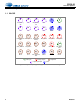
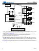
2 Typical Connection Diagram
2 Typical Connection Diagram
Figure 2-1. Typical Connection Diagram—Analog Microphone Connections
DMIC2_SCLK/
AD1
C1 30 VA I/O Digital MIC Interface 2 Serial Clock/
Address Select. High speed clock output
to the digital mics. Along with ASP_
SDOUT2/AD0, immediately sets the I
2
C
address when RESET
is deasserted.
Default is 0.
Weak
pulldown
CMOS
output
—Hi-Z
MUTE E6 16 VA I Mute. Asserting this pin mutes all four
channels. Also can be programmed to
power down modules as configured in the
MUTE pin control registers.
Weak
pulldown
— Hysteresis
on CMOS
input
—
VA A5 7
21
N/A I Analog/Digital Power. Power supply for
analog circuitry and digital circuitry via
internal LDO.
————
VP B6 10 N/A I Analog Power. Power supply for mic
bias.
————
GNDA B5 8 N/A I Analog Ground. Ground reference. — — — —
GNDD E4 20 N/A I Digital Ground. Ground reference. — — — —
Table 1-1. Pin Descriptions (Cont.)
Name
Ball
#
Pin
#
Power
Supply
I/O Description
Internal
Connection
Driver Receiver
State at
Reset
Power
CS53L30
GNDD
GNDA
DMIC1_SCLK
MIC1_BIAS
IN1
–
IN1+
MIC2_BIAS
IN2
–
IN2+
MIC3_BIAS
IN3
–
IN3+
MIC4_BIAS
IN4
–
IN4+
Analog Microphone Connection
Two-wire microphone connection
Rbias
Ground Ring
MICx_BIAS
INx+
INx–
Three-wire microphone connection
Ground Ring
MICx_BIAS
INx+
INx–
1 µF
C
INM
C
INM
Analog
Microphone
(see
connection
diagram)
1 µF
C
INM
C
INM
Analog
Microphone
(see
connection
diagram)
1 µF
C
INM
C
INM
Analog
Microphone
(see
connection
diagram)
1 µF
C
INM
C
INM
Analog
Microphone
(see
connection
diagram)
MIC_BIAS_FILT
*
4.7 µF
SYNC
SCL
SDA
SoC
VA
0.1 µF
R
P
*
R
P
+1.8 V +1.8 V
VP
0.1 µF
*
+3.6 V
FILT+
2.2 µF
*
PMU
ASP_LRCK/FSYNC
ASP_SCLK
ASP_SDOUT2/AD0
ASP_SDOUT1
MCLK
RESET
MUTE
R
P_I
Key for Capacitor Types Required:
* Use low ESR, X7R/X5R capacitors
All External Passive Component Values Shown Are Nominal Values.
DMIC2_SCLK/AD1
INT
Note 1
Note 3
Note 1
Note 3
Note 2
Note 2
Note 5
Note 4 Note 4
Note 7
Note 7
Note 2
Note 1
Note 3
Note 2
Note 1
Note 3
Note 6