
User Manual


DS992F1 41
CS53L30
5.3 Power-Down Sequence
5.3 Power-Down Sequence
Ex. 5-2 is a procedure for powering down the device.
9.4 Configure the ADC2A
and ADC2B preamp
and PGA settings.
ADC2A/2B AFE Control, Address 0x31–0x32
ADC2A AFE Control, Address 0x31 0x40
ADC2A_PREAMP[1:0]
†
ADC2A_PGA_VOL[5:0]
†
01
00 0000
ADC2A preamp gain is +10 dB.
ADC2A PGA is set to 0 dB.
ADC2B AFE Control, Address 0x32 0x40
ADC2B_PREAMP[1:0]
†
ADC2B_PGA_VOL[5:0]
†
01
00 0000
ADC2B preamp gain is +10 dB.
ADC2B PGA is set to 0 dB.
9.5 Configure the ADC2A
and ADC2B channel
volumes.
ADC2A/2B Digital Volume, Address 0x33–0x34
ADC2A Digital Volume, Address 0x33 0x00
ADC2A_VOL[7:0]
†
0000 0000 ADC2A digital volume is set to 0 dB.
ADC2B Digital Volume, Address 0x34 0x00
ADC2B_VOL[7:0]
†
0000 0000 ADC2B digital volume is set to 0 dB.
10 Write the following registers to power up the device.
STEP TASK REGISTER/BIT FIELDS VALUE DESCRIPTION
10.1 Enable TDM Mode. ASP Control 1, Address 0x0D 0x00
ASP_TDM_PDN
ASP_SDOUT1_PDN
ASP_3ST
SHIFT_LEFT
†
Reserved
ASP_SDOUT1_DRIVE
†
0
0
0
0
000
0
TDM Mode is enabled.
ASP_SDOUT1 output path is powered up.
ASP output clocks are active.
No shift.
—
The ASP_SDOUT1 pin has normal drive strength.
10.2 Power up the device. Power Control, Address 0x06 0x00
PDN_ULP
PDN_LP
DISCHARGE_FILT+
THMS_PDN
†
Reserved
0
0
0
0
0000
Ultralow power down is not enabled.
Power down is not enabled.
FILT+ pin is not clamped to ground.
Thermal sense is enabled.
—
†
Indicates bit fields for which the provided values are typical, but are not required for configuring the key functionality of the sequence. In the target
application, these fields can be set as desired without affecting the configuration goal of this start-up sequence.
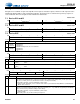
Example 5-2. Power-Down Sequence
STEP TASK
1 Write the following registers to mute the digital outputs.
STEP TASK REGISTER/BIT FIELDS VALUE DESCRIPTION
1.1 Mute Channels 1A
and 1B.
ADC1A/1B Digital Volume, Address 0x2B–0x2C
ADC1A Digital Volume, Address 0x2B 0x80
ADC1A_VOL[7:0] 1000 0000 ADC1A digital volume is set to mute.
ADC1B Digital Volume, Address 0x2C 0x80
ADC1B_VOL[7:0] 1000 0000 ADC1B digital volume is set to mute.
1.2 Mute Channels 2A
and 2B.
ADC2A/2B Digital Volume, Address 0x33–0x34
ADC2A Digital Volume, Address 0x33 0x80
ADC2A_VOL[7:0] 1000 0000 ADC2A digital volume is set to mute.
ADC2B Digital Volume, Address 0x34 0x80
ADC2B_VOL[7:0] 1000 0000 ADC2B digital volume is set to mute.
2 Read the interrupt status
register to clear any
previous PDN_DONE
interrupts.
REGISTER/BIT FIELDS VALUE DESCRIPTION
Device Interrupt Status, Address 0x36
PDN_DONE
THMS_TRIP
SYNC_DONE
ADC2B_OVFL
ADC2A_OVFL
ADC1B_OVFL
ADC1A_OVFL
MUTE_PIN
x
x
x
x
x
x
x
x
Indicates power down status.
Indicates thermal sense trip.
Indicates multichip synchronization sequence done.
Indicates overrange status in corresponding signal path.
Indicates overrange status in corresponding signal path.
Indicates overrange status in corresponding signal path.
Indicates overrange status in corresponding signal path.
Indicates MUTE pin assertion.
Example 5-1. Power-Up Sequence (Cont.)
STEP TASK