
User Manual


40 DS992F1
CS53L30
5.2 Power-Up Sequence
6.4 Configure TDM
channels.
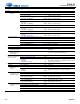
ASP TDM TX Control 1–4, Address 0x0E–0x11
ASP TDM TX Control 1, Address 0x0E 0x00
ASP_CH1_STATE
†
Reserved
ASP_CH1_TX_LOC[5:0]
†
0
0
00 0000
Channel 1 data is available.
—
Channel 1 begins at Slot 0.
ASP TDM TX Control 2, Address 0x0F 0x03
ASP_CH2_STATE
†
Reserved
ASP_CH2_TX_LOC[5:0]
†
0
0
00 0011
Channel 2 data is available.
—
Channel 2 begins at Slot 3.
ASP TDM TX Control 3, Address 0x10 0x06
ASP_CH3_STATE
†
Reserved
ASP_CH3_TX_LOC[5:0]
†
0
0
00 0110
Channel 3 data is available.
—
Channel 3 begins at Slot 6.
ASP TDM TX Control 4, Address 0x11 0x09
ASP_CH4_STATE
†
Reserved
ASP_CH4_TX_LOC[5:0]
†
0
0
00 1001
Channel 4 data is available.
—
Channel 4 begins at Slot 9.
6.5 Enable TDM slots. ASP TDM TX Enable 1–6, Address 0x12–0x17
ASP TDM TX Enable 1, Address 0x16 0x0F
ASP_TX_ENABLE1[7:0]
†
0000 1111 Slots 8-11 are enabled.
ASP TDM TX Enable 2, Address 0x17 0xFF
ASP_TX_ENABLE1[7:0]
†
1111 1111 Slots 0-7 are enabled.
7 Write the following registers to configure MUTE pin functionality.
STEP TASK REGISTER/BIT FIELDS VALUE DESCRIPTION
7.1 Configure MUTE pin
power down controls.
MUTE Pin Control 1, Address 0x1F
†
0x00 Default values (power down controls are not affected by
MUTE pin)
7.2 Configure MUTE pin
polarity and power
down controls.
MUTE Pin Control 2, Address 0x20
†
0x80 Default values (MUTE pin is active high, power down
controls are not affected by MUTE pin)
8 Write the following
registers to configure the
mic bias outputs.
REGISTER/BIT FIELDS VALUE DESCRIPTION
Mic Bias Control, Address 0x0A 0x06
MIC4_BIAS_PDN–MIC1_BIAS_PDN
†
Reserved
VP_MIN
†
MIC_BIAS_CTRL[1:0]
†
0000
0
1
10
All four mic bias outputs are enabled.
—
VP PSRR is optimized for a minimum voltage of 3.2 V.
Mic bias outputs are 2.75 V.
9 Write the following registers to configure the volume controls.
STEP TASK REGISTER/BIT FIELDS VALUE DESCRIPTION
9.1 Enable soft ramp on
digital volume
changes.
Soft Ramp Control, Address 0x1A 0x20
Reserved
DIGSFT
†
Reserved
00
1
0 0000
—
Digital volume changes occur with a soft ramp.
—
9.2 Configure the ADC1A
and ADC1B preamp
and PGA settings.
ADC1A/1B AFE Control, Address 0x29–0x2A
ADC1A AFE Control, Address 0x29 0x40
ADC1A_PREAMP[1:0]
†
ADC1A_PGA_VOL[5:0]
†
01
00 0000
ADC1A preamp gain is +10 dB.
ADC1A PGA is set to 0 dB.
ADC1B AFE Control, Address 0x2A 0x40
ADC1B_PREAMP[1:0]
†
01 ADC1B preamp gain is +10 dB.
ADC1B_PGA_VOL[5:0]
†
00 0000 ADC1B PGA is set to 0 dB.
9.3 Configure the ADC1A
and ADC1B channel
volumes.
ADC1A/1B Digital Volume, Address 0x2B–0x2C
ADC1A Digital Volume, Address 0x2B 0x00
ADC1A_VOL[7:0]
†
0000 0000 ADC1A digital volume is set to 0 dB.
ADC1B Digital Volume, Address 0x2C 0x00
ADC1B_VOL[7:0]
†
0000 0000 ADC1B digital volume is set to 0 dB.
Example 5-1. Power-Up Sequence (Cont.)
STEP TASK