
User Manual


DS992F1 37
CS53L30
4.15 QFN Thermal Pad
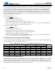
Figure 4-20. Control Port Timing, I
2
C Reads with Preamble and Autoincrement
The following pseudocode illustrates an aborted write operation followed by a single read operation. For multiple read
operations, autoincrement would be set on (as is shown in Fig. 4-20).
Send start condition.
Send 10010100 (chip address and write operation).
Receive acknowledge bit.
Send MAP byte, autoincrement off.
Receive acknowledge bit.
Send stop condition, aborting write.
Send start condition.
Send 10010101 (chip address and read operation).
Receive acknowledge bit.
Receive byte, contents of selected register.
Send acknowledge bit.
Send stop condition.
Note: The device interrupt status register (at address 0x36) and the register that immediately precedes it (the device
interrupt mask register at address 0x35) must only be read individually and not as a part of an autoincremented
control-port read. An autoincremented read of either register may clear the contents of the interrupt status register
and return invalid interrupt status data. If an unmasked interrupt condition had caused INT
to be asserted, INT
may be unintentionally deasserted.
Therefore, to avoid affecting interrupt status register contents, the autoincrement read must not include registers
at addresses 0x35 and 0x36; these registers must only be read individually.
4.15 QFN Thermal Pad
The underside of the compact QFN package reveals a large metal pad that serves as a thermal relief to provide for
maximum heat dissipation. Internal to the package, all grounds are connected to the thermal pad. This pad must mate with
an equally dimensioned copper pad on the PCB and must be electrically connected to ground. If necessary for thermal
reasons, a series of vias can be used to connect this copper pad to one or more larger ground planes on other PCB layers.
5 Systems Applications
This section describes the following system applications and considerations:
• Octal mic array application (Section 5.1)
• Power-up sequence (Section 5.2)
• Quick-mute sequencing (Section 5.3)
• Capture-path input considerations (Section 5.3)
• MCLK jitter (Section 5.5)
• Frequency response considerations (Section 5.6).
SCL
Chip Address (Write) MAP Byte Data
START
ACK
STOP
ACK
ACKACK
SDA
Chip Address (Read)
START
NO
16 8 9 12 13 14 15 4 5 6 7 0 1 20 21 22 23 24
26 27 28
2 3 10 11 17 18 19 25
ACK
STOP
MAP Addr = Z
INCR = 1
Addr = 1001010
R/W = 0
R/W = 1
Data Data
Data from
Addr Z
Data from
Addr Z+1
Data from
Addr Z+n
SDA
Source
Master Master Master
Pullup
Slave Slave
Slave Slave Slave
Master Master Master
Pullup
Addr = 1001010
643257106432571064325710707070