
User Manual


DS992F1 25
CS53L30
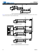
4.6 Serial Ports
4.6 Serial Ports
The CS53L30 has a highly configurable serial port to communicate audio and voice data to and from other devices in the
system such as application processors and bluetooth transceivers.
4.6.1 I/O
The serial port interface consists of four signals:
• ASP_SCLK. Serial data shift clock
• ASP_LRCK/FSYNC. Left/right (I
2
S) or frame sync clock (TDM)
• LRCK identifies the start of each serialized data word and locates the left and right channels within the data word
when I
2
S format is used (see Section 4.6.6).
• FSYNC identifies the start of each TDM frame.
• Toggles at external sample rate (Fs
ext
).
• ASP_SDOUTx. Serial data outputs
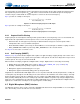
4.6.2 Serial Port Power-Up, Power-Down, and Tristate
The ASP has separate power-down and tristate controls for its output data paths. The serial port power, tristate, and TDM
control is done through ASP_3ST, ASP_TDM_PDN, and the respective ASP_SDOUTx_PDN bit. Separating power state
controls helps minimize power consumption when the output port is not in use.
• ASP_SDOUTx_PDN. If the SDOUT functionality of a serial port is not required, the SDOUT data path can be
powered down by setting ASP_SDOUTx_PDN. The ASP_SDOUTx pin is Hi-Z when ASP_SDOUTx_PDN is set; it
does not tristate the serial port clock.
• ASP_3ST. See Section 4.6.3 for details.
• ASP_TDM_PDN. When ASP_TDM_PDN = 1, the ASP serial port is configured to operate in I
2
S Mode. When ASP_
TDM_PDN = 0, ASP is configured to operate in TDM Mode and ASP_SDOUT2 is Hi-Z.
To facilitate clock mastering in TDM Mode, while not sending data, ASP_TDM_PDN and all ASP_TX_ENABLEy
bits must be cleared to prevent wasting power to drive the output nets. To save power when no TDM TX slots are
used, ASP_SDOUT1 is automatically tristated.
Master/slave operation is controlled only by the M/S
bit setting and is done irrespective of the setting of the ASP_SDOUTx_
PDN, and ASP_3ST bits.
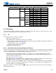
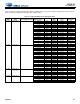
6.1440 0 X 2 3.0720 0
41.5360 1
1 8, 11.025,
12
20.7680 0
40.3840 1
16, 22.050,
24
21.5360 0
40.7680 1
32, 44.1, 48 2 3.0720 0
41.5360 1
6.4000 0 X 2 3.2000 0
41.6000 1
1 8, 11.025,
12
20.8000 0
40.4000 1
16, 22.050,
24
21.6000 0
40.8000 1
32, 44.1, 48 2 3.2000 0
41.6000 1
1.An X indicates that the sample rate setting does not affect DMICx_SCLK rate.
Table 4-1. Digital Mic Interface Clock Generation (Cont.)
Post-MCLK_DIV MCLK Rate
(MHz)
MCLK_INT_
SCALE
ASP_RATE
(kHz)
1
Divide
Ratio
DMICx_SCLK Rate
(MHz)
DMICx_SCLK_DIV
Programming