
User Manual


18 DS992F1
CS53L30
4 Functional Description
4 Functional Description
This section provides a general description of the CS53L30 architecture and detailed functional descriptions of the various
blocks that comprise the CS53L30.
4.1 Overview
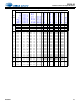
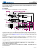
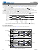
Fig. 4-1 is a block diagram of the CS53L30 with links to descriptions of major subblocks.
Figure 4-1. Overview of Signal Flow
The CS53L30 is a low-power, four-channel, 24-bit audio ADC. The ADCs are fed by fully differential analog inputs that
support mic and line-level input signals. The ADCs are designed using multibit delta-sigma techniques. The ADCs operate
at an optimal oversampling ratio balancing performance with power savings. Enhanced power savings are possible when
the internal MCLK is scaled by setting MCLK_INT_SCALE (see p. 45). Table 4-2 lists supported sample rates with scaled
internal MCLK.
The serial data port operates at a selectable range of standard audio sample rates as either timing master or slave. Core
timing is flexibly sourced, without the need of a PLL, by clocks with typical audio clock rates (N x 5.6448, or N x 6.1440
MHz; where N = 1 or 2), USB rates (6 or 12 MHz), or 3G and DVB rates (19.2 MHz).
The integrated LDO regulator allows the digital core to operate at a very low voltage, significantly reducing the CS53L30’s
overall power consumption.
The CS53L30 can operate in a system with multiple CS53L30s to increase the number of channels available. The
CS53L30s may be connected in a multidrop configuration in TDM Mode. Up to four CS53L30s can operate simultaneously
on the same TDM bus. Connecting together the SYNC pins of multiple CS53L30s allows operation with minimal
channel-to-channel phase mismatch across devices.
The signal to be converted can be either mic/line-level. The digital mic inputs (IN1+/DMIC1_SD, IN3+/DMIC2_SD) connect
directly to the decimators.
CS53L30
Digital Processing
Control
Port
Level Shifters
MIC 1_BIAS
Serial Port
MIC 2_BIAS
VP
MCLK
DMIC1_SCLK
MIC3_BIAS
MIC4_BIAS
–6 to +12 dB,
0.5 dB steps
+10 or +20 dB
ADC1B
–
+
–
+
Decimators
–6 to +12 dB,
0.5 dB steps
+10 or +20 dB
–
+
–
+
Decimators
MIC1 Bias
MIC2 Bias
MIC3 Bias
MIC4 Bias
HPF, Noise
Gate, Volume,
Mute
Audio
Serial Port
Control Port
RESET
MCLK_INT
Clock Divider
Synchronizer
DMIC
ADC1A
ADC2B
ADC2A
–
+
–
+
LDO
VA
VD
2
2
4
MCLK_INT
MCLK_INT
HPF, Noise
Gate, Volume,
Mute
SYNC
MUTE
Synchronous
SRC
IN1+/DMIC1_SD
IN2–
IN1–
IN2+
IN3+/DMIC2_SD
IN4–
IN3–
IN4+
DMIC2_SCLK
See Section 4.4.
See
Section 4.9.
See Section 4.5.
See Section 4.6.
See
Section 4.8.
See Section 4.14.
See Section 4.12.
See Section 4.2.