
User Manual


DS992F1 17
CS53L30
3 Characteristics and Specifications
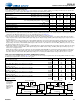
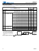
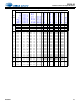
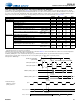
Table 3-14. Digital Interface Specifications and Characteristics
Test conditions (unless specified otherwise): Fig. 2-1 shows CS53L30 connections; GNDA = GNDD = 0 V; all voltages are with respect to ground;
VA =1.8 V, VP = 3.6 V; T
A
= +25°C
Parameters
1
1.See Table 1-1 for serial and control port power rails.
Symbol Min Max Units
Input leakage current
2
2.Specification is per pin. Includes current through internal pull-down resistors on serial port.
MCLK, SYNC, MUTE, all serial port inputs
All control port inputs, INT,
RESET
I
in
—
—
±4000
±100
nA
nA
Internal weak pulldown — 550 2450 k
Input capacitance
2
—— 10pF
INT
current sink (V
OL
= 0.3 V max) — 825 — µA
High-level output voltage
3
3.I
OH
= –100 µA for x_DRIVE = 0; I
OH
= –67 µA for x_DRIVE = 1
V
OH
VA – 0.2 — V
Low-level output voltage
4
4.I
OL
= 100 µA for x_DRIVE = 0; I
OL
= 67 µA for x_DRIVE = 1
V
OL
—0.2V
High-level input voltage V
IH
0.70•VA — V
Low-level input voltage V
IL
—0.30•VAV
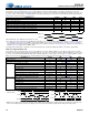
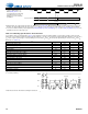
Table 3-15. Thermal Overload Detection Characteristics
Test conditions (unless otherwise specified): GNDA = GNDD = 0; all voltages are with respect to ground; VA = 1.8 V, VP = 3.6 V.
Parameters Min Typ Max Units
Thermal overload detection threshold — 150 —
C