
User Manual


16 DS992F1
CS53L30
3 Characteristics and Specifications
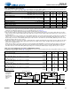
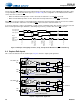
8.Hand-off timing for multidevice
systems (SHIFT_LEFT = 1).
When SHIFT_LEFT = 1, it is
recommended to insert an empty
slot between devices on the
TDM bus to prevent contention
possibilities.
9.In Master Mode, the output sample rate follows the MCLK rate, per Section 4.6.5. MCLK deviations from the nominal supported rates are passed
directly to the output sample rate by the same factor (e.g., a +100 ppm offset in the frequency of MCLK becomes a +100 ppm offset in FSYNC).
10.“n” refers to number of SCLK cycles programmed in LRCK_TPWH[10:3] | LRCK_TPWH[2:0] (see p. 51) when
LRCK_50_NPW (see p. 51) is set;
otherwise, t
FSYNC
has a 50% duty cycle.
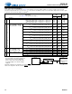
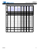
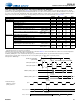
Table 3-13. Switching Specifications—I
2
C Control Port
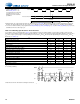
Test conditions (unless specified otherwise): Fig. 2-1
shows CS53L30 connections
; GNDA = GNDD = 0 V; all voltages are with respect to ground;
Parameters can vary with VA, typical performance data taken with VA = 1.8 V, VP = 3.6 V, min/max performance data taken with VA = 1.8V, VP = 3.6V;
T
A
= +25°C; logic 0 = ground, logic 1 = VA; input timings are measured at V
IL
and V
IH
thresholds, and output timings are measured at V
OL
and V
OH
thresholds (see Table 3-14).
Parameter
1,2
1.All specifications are valid for the signals at the pins of the CS53L30 with the specified load capacitance.
2.I
2
C control port timing.
Symbol Min Max Unit
RESET
rising edge to start
t
irs
500 — ns
SCL clock frequency f
scl
— 550 kHz
Start condition hold time (prior to first clock pulse) t
hdst
0.6 — µs
Clock low time t
low
1.3 — µs
Clock high time t
high
0.6 — µs
Setup time for repeated start condition t
sust
0.6 — µs
SDA input hold time from SCL falling
3
3.Data must be held for sufficient time to bridge the transition time, t
f
, of SCL.
t
hddi
00.9µs
SDA output hold time from SCL falling t
hddo
0.2 0.9 µs
SDA setup time to SCL rising t
sud
100 — ns
Rise time of SCL and SDA t
rc
— 300 ns
Fall time SCL and SDA t
fc
— 300 ns
Setup time for stop condition t
susp
0.6 — µs
Bus free time between transmissions t
buf
1.3 — µs
SDA bus capacitance C
L
— 400 pF
SDA pull-up resistance R
p
500 —
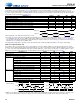
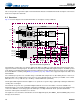
SLOTx:LSB+1
SCLK
Device 0: SDOUT
t
HOLD2
SLOTx:LSB
SLOTx:MSB
SLOTx:MSB -1
SLOTx:MSB -2
Output Not Driven (Hi-Z)
Output Not Driven (Hi-Z)
t
buf
t
hdst
t
hdst
t
low
t
r
t
f
t
hdd
t
high
t
sud
t
sust
t
susp
Stop Start
Start
Stop
Repeated
SDA
SCL
t
irs
RESET