
User Manual


DS992F1 15
CS53L30
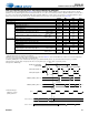
3 Characteristics and Specifications
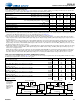
Table 3-12. Switching Specifications—Time-Division Multiplexed (TDM) Mode
Test conditions (unless specified otherwise): Fig. 2-1 shows CS53L30 connections; GNDA = GNDD = 0 V; all voltages are with respect to ground;
parameters can vary with VA; typical performance data taken with VA = 1.8 V, VP = 3.6 V; min/max performance data taken with VA = 1.8 V, VP = 3.6 V;
T
A
= +25°C; Test load for ASP_LRCK/FSYNC, ASP_SCLK, and ASP_SDOUT1 C
L
= 60 pF; logic 0 = ground, logic 1 = VA; ASPx_DRIVE = 0; input
timings are measured at V
IL
and V
IH
thresholds, and output timings are measured at V
OL
and V
OH
thresholds (see Table 3-14).
Parameters Symbol Min Max Units
MCLK frequency — 1.024 19.2 MHz
MCLK duty cycle —45 55 %
Slave mode Input sample rate (FSYNC)
1,2
1.Clock rates must be stable when the device is powered up and the serial port is not powered down. Therefore, the appropriate serial port must be
powered down before any clock rates are changed.
2.Maximum frequency for the highest supported nominal rate is indicated.
Table 4-2 shows nominal MCLK rates and their associated configurations.
Fs
ext
—48kHz
FSYNC high time pulse
3
3.“n” refers to the total number of SCLKs in one FSYNC frame.
t
FSYNC
1/f
SCLK
(n–1)/f
SCLK
s
FSYNC setup time before SCLK rising edge t
SETUP1
20 — ns
SCLK frequency
4,5
4.If MCLK_19MHZ_EN is set, the maximum SCLK frequency is 6.4 MHz. If SHIFT_LEFT is set, the maximum SCLK frequency is 6.4 MHz.
5.SCLK frequency must be high enough to provide the necessary SCLK cycles to capture all the serial audio port bits.
f
SCLK
—12.288MHz
SCLK duty cycle — 45 55 %
SDOUT delay time after SCLK rising edge
6
6.Single-device TDM timings
SHIFT_LEFT = 0 t
CLK-Q1
—25ns
SHIFT_LEFT = 1 t
CLK-Q1
—45ns
SDOUT hold time of LSB before transition to Hi-Z SHIFT_LEFT = 0
[7]
7.Hand-off timing for
multidevice systems
(SHIFT_LEFT = 0.
t
HOLD2
10 30 ns
SHIFT_LEFT = 1
[8]
t
HOLD2
10 40 ns
Master mode Output sample rate (FSYNC)
1
Fs
ext
—
[9]
kHz
FSYNC high time pulse
10
t
FSYNC
1/f
SCLK
(n–1)/f
SCLK
s
FSYNC setup time before SCLK rising edge t
SETUP1
15 — ns
SCLK frequency f
SCLK
(See Table 4-3)MHz
SCLK duty cycle — 45 55 %
SDOUT delay time after SCLK rising edge SHIFT_LEFT = 0 t
CLK-Q1
—25ns
SDOUT delay time after SCLK rising edge
6
SHIFT_LEFT = 1 t
CLK-Q2
—45ns
SDOUT hold time of LSB before transition to Hi-Z SHIFT_LEFT = 0
[7]
t
HOLD2
10 30 ns
SHIFT_LEFT = 1
[8]
t
HOLD2
10 40 ns
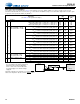
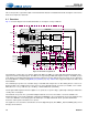
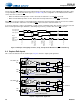
//
//
//
//
//
SLOT0:MSB
FSYNC (programmable
pulse width)
SCLK (SCLK_INV = 0)
SDOUT (SHIFT_LEFT = 0)
//
//
//
//
//
//
t
setup1
t
Fsync
t
CLK-Q1
SLOT0:MSB -1
//
//
//
SLOT0:MSB
SDOUT (SHIFT_LEFT = 1)
//
//
t
CLK-Q1
SLOT0:MSB -1
//
//
SLOT0:MSB -2
//
//
SCLK (SCLK_INV = 1)
//
//
//
//
//
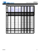
SLOTx:LSB+1
SCLK
Device 0: SDOUT
t
HOLD2
SLOTx:LSB
SLOTx:MSB
Device 1: SDOUT
SLOTx:MSB -1
SLOTx:MSB -2
Output Not Driven (Hi-Z)
Output Not Driven (Hi-Z)