
User Manual


14 DS992F1
CS53L30
3 Characteristics and Specifications
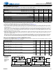
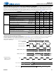
Table 3-10. Switching Specifications—Digital Mic Interface
Test conditions (unless specified otherwise): Fig. 2-1
shows CS53L30 connections
; GNDA = GNDD = 0 V; voltages are with respect to ground;
parameters can vary with VA, typical performance data taken with VA = 1.8 V, VP = 3.6 V, min/max performance data taken with VA = 1.8 V, VP = 3.6 V;
T
A
= +25°C; logic 0 = ground, logic 1 = VA; DMIC_DRIVE = 0 (normal); input timings are measured at V
IL
and V
IH
thresholds, and output timings are
measured at V
OL
and V
OH
thresholds (see Table 3-14).
Parameters
1,2
1.Digital mic interface timing
2.Oversampling rate of the digital mic must match the oversampling rate of the CS53L30 internal decimators.
Symbol Min Max Units
Output clock (DMICx_SCLK) frequency 1/t
P
—3.2
[3]
3.The output clock frequency follows the internal MCLK rate divided by 2 or 4, as set in the ADCx/DMICx control registers (see DMIC1_SCLK_DIV on
p. 53 and DMIC2_SCLK_DIV on p. 55). DMICx_SCLK is further divided by up to a factor of 4 when MCLK_INT_SCALE is set (see p. 48). MCLK
source deviation from nominal supported rates is applied directly to the output clock rate by the same factor (e.g., a +100-ppm offset in the frequency
of MCLK becomes a +100-ppm offset of DMICx_SCLK.
MHz
DMICx_SCLK duty cycle
4
—45 55%
DMICx_SCLK rise time (10% to 90% of VA)
4
4.Timing guaranteed with pull-up or pull-down resistor, with a minimum value 10 ktied to DMIC2_SCLK/AD1 for I
2
C address determination.
t
r
—21ns
DMICx_SCLK fall time (90% to 10% of VA)
4
t
f
—13ns
DMICx_SD setup time before DMICx_SCLK rising edge t
s(SD-CLKR)
10 — ns
DMICx_SD hold time after DMICx_SCLK rising edge t
h(CLKR-SD)
4—ns
DMICx_SD setup time before DMICx_SCLK falling edge t
s(SD-CLKF)
10 — ns
DMICx_SD hold time after DMICx_SCLK falling edge t
h(CLKF-SD)
4—ns
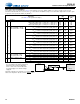
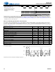
Table 3-11. Specifications—I
2
S
Test conditions (unless specified otherwise): Fig. 2-1 shows CS53L30 connections; GNDA = GNDD = 0 V; all voltages are with respect to ground;
parameters can vary with VA; typical performance data taken with VA = 1.8 V, VP = 3.6 V; min/max performance data taken with VA = 1.8 V, VP = 3.6 V;
T
A
= +25°C; Test load for ASP_LRCK/FSYNC, ASP_SCLK, and ASP_SDOUTx C
L
= 60 pF; logic 0 = ground, logic 1 = VA; ASPx_DRIVE = 0; input
timings are measured at V
IL
and V
IH
thresholds, and output timings are measured at V
OL
and V
OH
thresholds (see Table 3-14).
Parameters
1,2
1.Serial port
interface timing
2.MCLK must be stable before powering up the device. In Slave Mode, ASP_LRCK/FSYNC and ASP_SCLK must be stable before powering up the
device. Before making changes to any clock setting, the device must be powered down by setting either the PDN_ULP or PDN_LP bit.
Symbol Min Max Units
MCLK frequency — 1.024 19.2 MHz
MCLK duty cycle — 45 55 %
Slave mode Input sample rate (LRCK) Fs (See Table 4-2)kHz
LRCK duty cycle — 45 55 %
SCLK frequency 1/t
Ps
— 64•Fs
ext
Hz
SCLK duty cycle — 45 55 %
SCLK rising edge to LRCK edge t
hs(LK-SK)
10 — ns
LRCK setup time before SCLK rising edge t
ss(LK-SK)
40 — ns
SDOUT setup time before SCLK rising edge t
ss(SDO-SK)
20 — ns
SDOUT hold time after SCLK rising edge t
hs(SK-SDO)
30 — ns
Master mode Output sample rate (LRCK) All speed modes Fs
ext
(See Table 4-2)kHz
LRCK duty cycle — 45 55 %
SCLK frequency 1/t
Pm
— 64•Fs
ext
Hz
SCLK duty cycle — 33 67 %
LRCK time before SCLK falling edge t
sm(LK-SK)
–2 +2 ns
SDOUT setup time before SCLK rising edge t
sm(SDO-SK)
20 — ns
SDOUT hold time after SCLK rising edge t
hm(SK-SDO)
30 — ns
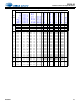
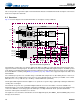
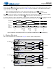
DMIC_CLK
DMIC_SD
Left
(A, DATA1)
Channel Data
Right
(B, DATA2)
Channel Data
Left
(A, DATA1)
Channel Data
t
hm(SK-SDO)
//
//
//
//
//
//
MSB
LRCK
SCLK
SDOUT
t
Pm
t
sm(SDO-SK)
//
//
//
//
//
//
t
sm(LK-SK)
t
hs(SK-SDO)
//
//
//
//
//
//
MSB
LRCK
SCLK
SDOUT
t
ss(LK-SK)
t
P
t
ss(SDO-SK)
//
//
//
//
//
//
t
hs(LK-SK)
Serial Port Timing—Master Mode
Serial Port Timing—Slave Mode