
User Manual


DS992F1 11
CS53L30
3 Characteristics and Specifications
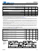
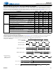
Table 3-6. MIC BIAS Characteristics
Test conditions (unless otherwise specified): Fig. 2-1 shows CS53L30 connections; GNDA = GNDD = 0; all voltages are with respect to ground; VA =
1.8 V, VP = 3.6 V, T
A
= +25°C; only one bias output is powered up at a time; MCLK_INT_SCALE = 0.
Parameters Min Typ Max Units
Output voltage
1
1.The output voltage includes attenuation due to the MIC BIAS output resistance (R
OUT
).
MIC_BIAS_CTRL = 01 (1.8-V mode)
MIC_BIAS_CTRL = 10 (2.7-V mode)
1.71
2.61
1.80
2.75
1.89
2.86
V
V
Mic bias startup delay
2
2.Startup delay times are approximate and vary with MCLK
INT
frequency. If MCLK_INT_SCALE = 1, the startup delay time is scaled up by the MCLK
INT
scaling factor. The MCLK
INT
scaling factor is 1, 2, or 4, depending on Fs
EXT
. See Table 4-2.
—10—ms
Rise time
3
3.From 10% to 90% of typical output voltage. External capacitor on MICx_BIAS is as shown in Fig. 2-1.
I
OUT
= 500 µA, MIC_BIAS_CTRL = 01 (1.8-V mode)
I
OUT
= 500 µA, MIC_BIAS_CTRL = 10 (2.7-V mode)
I
OUT
= 2 mA
—
—
—
0.2
0.5
—
—
—
3
ms
ms
ms
DC output current (I
OUT
) Per output — — 2 mA
Integrated output noise f = 100 Hz–20 kHz — 3 — µVrms
Dropout voltage
4
4.Dropout voltage indicates the point where an output’s voltage starts to vary significantly with reductions to its supply voltage. When the VP supply
voltage drops below the programmed MICx_BIAS output voltage plus the dropout voltage, the MICx_BIAS output voltage progressively decreases as
its supply decreases.
Dropout voltage is measured by reducing the VP supply until MICx_BIAS drops 10 mV from its initial voltage with the default typical test condition VP
voltage (= 3.6 V, as in test conditions listed above). The difference between the VP supply voltage and the MICx_BIAS voltage at this point is the
dropout voltage. For instance, if the initial MICx_BIAS output is 2.86 V when VP = 3.6 V and VP = 3.19 V when MICx_BIAS drops to 2.85 V (–10 mV),
the dropout voltage is 340 mV (3.19 V – 2.85 V).
— — 340 mV
PSRR reduction voltage
5
5.PSRR voltage indicates the point where an output’s supply PSRR starts to degrade significantly with supply voltage reductions. When the VP supply
voltage drops below the programmed MICx_BIAS output voltage plus the PSRR reduction voltage, the MICx_BIAS output’s PSRR progressively
decreases as its supply decreases.
PSRR reduction voltage is measured by reducing the VP supply until MICx_BIAS PSRR @ 217 Hz falls below 100 dB. The difference between the
VP supply voltage and the MICx_BIAS voltage at this point is the PSRR reduction voltage. For instance, if the MICx_BIAS PSRR falls to 99.9 dB
when VP is reduced to 3.25 V and the MICx_BIAS output voltage is 2.75 V at that point, PSRR reduction voltage is 500 mV (3.25 V – 2.75 V).
— — 500 mV
Output resistance (R
OUT
) I
OUT
= 2-mA — 30 —
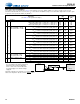
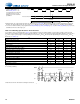
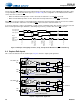
Table 3-7. Power-Supply Rejection Ratio (PSRR) Characteristics
Test conditions (unless specified otherwise): Fig. 2-1 shows CS53L30 connections; input test signal held low (all zero data); GNDA = GNDD = 0; voltages
are with respect to ground; VA = 1.8 V, VP = 3.6 V; T
A
= +25°C.
Parameters
1
1.PSRR test
configuration:
Typical PSRR
can vary by
approximately
6 dB below the
indicated
values.
Min Typical Max Units
INx (32-dB analog gain)
PSRR with 100-mVpp signal AC coupled to VA supply
217 Hz
1kHz
20 kHz
—
—
—
70
70
55
—
—
—
dB
dB
dB
MICx_BIAS (MICx_BIAS = 2.7-V mode, I
OUT
= 500 µA)
PSRR with 100 mVpp signal AC coupled to VA supply
VP_MIN = 0 (3.0 V)
217 Hz
1kHz
20 kHz
—
—
—
105
100
95
—
—
—
dB
dB
dB
MICx_BIAS (MICx_BIAS = 2.7-V mode, I
OUT
= 500 µA)
PSRR with 100 mVpp signal AC coupled to VA supply
VP_MIN = 1 (3.2 V)
217 Hz
1kHz
20 kHz
—
—
—
105
100
95
—
—
—
dB
dB
dB
MICx_BIAS (MICx_BIAS = 2.7-V mode, I
OUT
= 500 µA)
PSRR with 100 mVpp signal AC coupled to VP supply
VP_MIN = 0 (3.0 V)
217 Hz
1kHz
20 kHz
—
—
—
90
90
70
—
—
—
dB
dB
dB
MICx_BIAS (MICx_BIAS = 2.7-V mode, I
OUT
= 500 µA)
PSRR with 1 Vpp signal AC coupled to VP supply
VP_MIN = 1 (3.2 V)
217 Hz
1kHz
20 kHz
—
—
—
120
115
105
—
—
—
dB
dB
dB
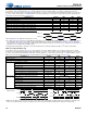
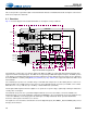
Operational
Amplifier
OUT
GND
Power DAC
OUT
GND
PWR
DUT
+5V +5V
++––
+
–
OUT
Analog Generator Analog Analyzer
Analog Test Equipment
Analog Output PSRR
Operational
Amplifier
OUT
GND
Power DAC
SDOUT
GND
PWR
DUT
+5V +5V
+–
+
–
OUT
Analog Generator Analog Analyzer
Test Equipment
Digital Output PSRR
Digital Analyzer