
User Manual

10 DS992F1
CS53L30
3 Characteristics and Specifications
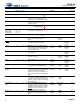
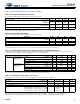
Table 3-5. Analog-Input-to-Serial-Port Characteristics
Test conditions (unless otherwise specified): Fig. 2-1 shows CS53L30 connections; input is a full-scale 1-kHz sine wave; ADCx_PREAMP = +10 dB; ADCx_PGA_
VOL = 0 dB; GNDA = GNDD = 0; voltages are
with respect to ground; parameters can vary with VA, typical performance data taken with VA = 1.8 V, VP = 3.6 V,
min/max performance data taken with
V
A = 1.8 V, VP = 3.6 V; T
A
= +25°C; measurement bandwidth is 20 Hz–20 kHz; LRCK = Fs = 48 kHz.
Parameters
1
1.Measures are referred to the applicable typical full-scale voltages. Applies to all THD+N and dynamic range values in the table.
Min Typ Max Units
Dynamic range
2
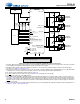
2.INx dynamic range test configuration (pseudodifferential) Includes noise from MICx_BIAS
output (2.7-V setting) through a series 2.21-k resistor connected to INx. Input signal is –60 dB
down from the corresponding full-scale signal input voltage.
Preamp setting: Bypass, PGA setting: 0 dB A-weighted
unweighted
87
85
93
91
—
—
dB
dB
Preamp setting: Bypass, PGA setting: +12 dB A-weighted
unweighted
80
78
86
84
—
—
dB
dB
Preamp setting: +10 dB, PGA setting: 0 dB A-weighted
unweighted
84
82
90
88
—
—
dB
dB
Preamp setting: +10 dB, PGA setting: +12 dB A-weighted
unweighted
74
72
80
78
—
—
dB
dB
Preamp setting: +20 dB, PGA setting: 0 dB A-weighted
unweighted
78
76
84
82
—
—
dB
dB
Preamp setting: +20 dB, PGA setting: +12 dB A-weighted
unweighted
66
64
72
70
—
—
dB
dB
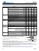
Total harmonic
distortion + noise
3
3.Input signal amplitude is relative to typical full-scale signal input voltage.
Preamp setting: Bypass, PGA setting: 0 dB –1 dB — –84 –78 dB
Preamp setting: Bypass, PGA setting: +12 dB –1 dB — –80 –74 dB
Preamp setting: +10 dB, PGA setting: 0 dB –1 dB — –76 –70 dB
Preamp setting: +10 dB, PGA setting: +12 dB –1 dB — –63 –57 dB
Preamp setting: +20 dB, PGA setting: 0 dB –1 dB — –70 –64 dB
Preamp setting: +20 dB, PGA setting: +12 dB –1 dB — –62 –56 dB
Common-mode rejection
4
4.INx CMRR test configuration
—70—dB
DC accuracy Interchannel gain mismatch
5
5.Measurements taken at all defined full-scale signal input voltages.
—±0.2— dB
Gain drift
5
— ±100 — ppm/°C
PGA A/B gain G
MIN
G
MAX
G
–6.25
11.75
0.375
–6
12
0.5
–5.75
12.25
0.625
dB
dB
dB
Preamp A/B gain G
MIN
G
MAX
9.5
19.9
10
20
10.5
20.5
dB
dB
Offset error
6
6.SDOUT code with ADC_HPF_EN = 1, DIG_BOOSTx = 0. The offset is added at the ADC output; if two ADC sources are mixed, their offsets add.
—
128
—LSB
Phase accuracy Multichip interchannel phase mismatch
7
7.Measured between two CS53L30 chips with input pairs IN1 selected and driven from same source with an MCLK of 19.2 MHz, 16-kHz sample rate,
and 8-kHz full-scale sine wave with preamp gain of +20 dB and PGA gain of +12 dB.
—
0.5
—
°
Interchannel phase mismatch
8
8.Measured between input pairs (IN1 to INx, IN2 to INx, IN3 to INx, IN4 to INx) with +20 dB preamp gain and +12 dB PGA gain.
—
0.5
—
°
Input Interchannel isolation
8
217 Hz
1kHz
20 kHz
—
—
—
90
90
80
—
—
—
dB
dB
dB
Full-scale signal
input voltage
9
9.ADC full-scale input voltage is measured between INx+ and INx– with the preamp set to bypass and the PGA set to 0-dB gain. Maximum input signal
level for INx depends on the preamp and PGA gain settings described in Section 5.4.1. The digital output level corresponding to ADC full-scale input
is less than 0 dBFS due to signal attenuation through the SRC; see Table 4-4.
Preamp setting: 0 dB, PGA setting: 0 dB
Preamp setting: +10 dB, PGA setting: 0 dB
Preamp setting: +10 dB, PGA setting: +12 dB
Preamp setting: +20 dB, PGA setting: 0 dB
Preamp setting: +20 dB, PGA setting: +12 dB
0.78•VA
—
—
—
—
0.82•VA
0.258•VA
0.064•VA
0.081•VA
0.020•VA
0.88•VA
—
—
—
—
Vpp
Vpp
Vpp
Vpp
Vpp
Input impedance
10
10.Measured between INx+ and INx–.
Preamp setting: 0 dB
Preamp setting: +10 or +20 dB;
45
0.9
50
1
—
—
k
M
DC voltage at INx
(pin floating)
11,12
11.INx pins are biased as specified when weak VCM is selected in the input bias control registers; see Section 7.19 and Section 7.20.
12.Changing gain settings to Bypass Mode may cause audible artifacts due to the difference in DC operating points between modes.
Preamp setting: Bypass ADCx_PDN = 0
ADCx_PDN = 1
—
—
0.42•VA
0.50•VA
—
—
V
V
Preamp setting: +10 dB or +20 dB ADCx_PDN = 0
ADCx_PDN = 1
—
—
0.39•VA
0.50•VA
—
—
V
V
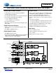
–60 dB,
1 kHz
INx+
INx–
MICx_BIAS
2.21 k
2.21 k
0.1 µF
0.1 µF
100 mV
PP
, 25 Hz
0.1 µF
INx+
INx–