CS53L30 Low-Power Quad-Channel Microphone ADC with TDM Output Analog Input and ADC Features System Features 91-dB dynamic range (A-weighted) @ 0-dB gain Native (no PLL required) support for 6-/12-MHz, 6.144-/ 12.288-MHz, 5.6448-/11.2896-MHz, or 19.2-MHz master clock rates and 8- to 48-kHz audio sample rates –84-dB THD+N @ 0-dB gain Four fully differential inputs: Four analog mic/line inputs Four analog programmable gain amplifiers –6 to +12 dB, in 0.5-dB steps Master or Slave Mode.
CS53L30 General Description The CS53L30 is a high-performance, low-power, quad-channel ADC. It is designed for use in multiple-mic applications while consuming minimal board space and power. The flexible ADC inputs can accommodate four channels of analog mic or line-input data in differential, pseudodifferential, or single-ended mode, or four channels of digital mic data. The analog input path includes a +10- to +20-dB boost and a –6- to +12-dB PGA.
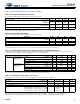
CS53L30 Table of Contents 1 Pin Descriptions . . . . . . . . . . . . . . . . . . . . . . . . . . . . . . . . . . . . . . 4 1.1 WLCSP . . . . . . . . . . . . . . . . . . . . . . . . . . . . . . . . . . . . . . . . . . 4 1.2 QFN . . . . . . . . . . . . . . . . . . . . . . . . . . . . . . . . . . . . . . . . . . . . 5 1.3 Pin Descriptions . . . . . . . . . . . . . . . . . . . . . . . . . . . . . . . . . . . 5 2 Typical Connection Diagram . . . . . . . . . . . . . . . . . . . . . . . . . . .
CS53L30 1 Pin Descriptions 1 Pin Descriptions 1.
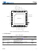
CS53L30 1.2 QFN IN1– IN1+/DMIC1_SD DMIC2_SCLK/AD1 DMIC1_SCLK ASP_SDOUT1 ASP_SCLK MCLK SDA 1.2 QFN 32 31 30 29 28 27 26 25 IN2+ 1 24 SCL IN2– 2 23 ASP_SDOUT2/AD0 IN3+/DMIC2_SD 3 22 ASP_LRCK/FSYNC IN3– 4 21 VA Thermal Pad 19 SYNC VA 7 18 RESET GNDA 8 17 INT 11 12 13 14 15 16 MUTE 10 MIC1_BIAS 9 MIC_BIAS_FILT 6 MIC4_BIAS IN4– MIC3_BIAS GNDD MIC2_BIAS 20 VP 5 FILT+ IN4+ Figure 1-2. Top-Down (Through-Package) View—32-Pin QFN Package 1.
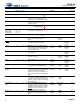
CS53L30 1.3 Pin Descriptions Table 1-1. Pin Descriptions (Cont.) Name Ball Pin # # Power I/O Supply Description Internal Connection Driver Receiver State at Reset — — — — — — — — — — — Hi-Z Filter pins MIC_BIAS_FILT D6 15 VP I Microphone Bias Voltage Filter. Filter connection for the internal quiescent voltage used for the MICx_BIAS outputs. FILT+ A6 9 VA O Positive Reference Filter. Positive reference voltage filter for internal sampling circuits.
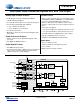
CS53L30 2 Typical Connection Diagram Table 1-1. Pin Descriptions (Cont.) Ball Pin # # Name Power I/O Supply DMIC2_SCLK/ AD1 C1 30 VA MUTE E6 16 VA Description I/O Digital MIC Interface 2 Serial Clock/ Address Select. High speed clock output to the digital mics. Along with ASP_ SDOUT2/AD0, immediately sets the I2C address when RESET is deasserted. Default is 0. I Mute. Asserting this pin mutes all four channels.
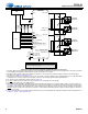
CS53L30 2 Typical Connection Diagram CS53L30 PMU MIC1_BIAS FILT+ +1.8 V +1.8 V 0.47 µF +3.6 V L /R DATA VP 0.1 µF Left Digital Microphone 1 * VA 0.1 µF Note 4 R P_ I Note 4 RP * RP DMIC1_SCLK IN1+/DMIC1_SD 0.47 µF DATA L/ R Right Digital Microphone 1 SCL SDA MIC3_BIAS INT Note 6 RESET 0.47 µF MCLK SoC L /R DATA ASP_LRCK/FSYNC Left Digital Microphone 2 ASP_SCLK ASP_SDOUT2/AD0 Note 7 ASP_SDOUT1 MUTE 0.
CS53L30 3 Characteristics and Specifications 3 Characteristics and Specifications Section 8 provides additional details about parameter definitions. Table 3-1. Recommended Operating Conditions Test conditions: GNDA = GNDD = 0 V; all voltages are with respect to ground. Parameters 1 DC power supply Symbol VA VP Analog/Digital VP_MIN = 1 VP_MIN = 0 VA domain pins VP domain pins Commercial External voltage applied to pin 2 Ambient temperature Min 1.71 3.2 3.0 –0.3 –0.3 –10 VIN-AI VIN-PI TA Max 1.89 5.
CS53L30 3 Characteristics and Specifications Table 3-5. Analog-Input-to-Serial-Port Characteristics Test conditions (unless otherwise specified): Fig. 2-1 shows CS53L30 connections; input is a full-scale 1-kHz sine wave; ADCx_PREAMP = +10 dB; ADCx_PGA_ VOL = 0 dB; GNDA = GNDD = 0; voltages are with respect to ground; parameters can vary with VA, typical performance data taken with VA = 1.8 V, VP = 3.6 V, min/max performance data taken with VA = 1.8 V, VP = 3.
CS53L30 3 Characteristics and Specifications Table 3-6. MIC BIAS Characteristics Test conditions (unless otherwise specified): Fig. 2-1 shows CS53L30 connections; GNDA = GNDD = 0; all voltages are with respect to ground; VA = 1.8 V, VP = 3.6 V, TA = +25°C; only one bias output is powered up at a time; MCLK_INT_SCALE = 0. Parameters Output voltage 1 Min 1.71 2.61 — — — — — — — — — MIC_BIAS_CTRL = 01 (1.8-V mode) MIC_BIAS_CTRL = 10 (2.
CS53L30 3 Characteristics and Specifications Table 3-8. Power Consumption Test conditions (unless specified otherwise): Fig. 2-1 shows CS53L30 connections; GNDA = GNDD = 0 V; voltages are with respect to ground; performance data taken with VA = 1.8 V, VP = 3.6 V; TA = +25°C; MCLK = 12.288 MHz; serial port set to Slave Mode; digital volume = 0 dB; no signal on any input; control port inactive; MCLK_INT_SCALE = 1. Use Cases 1 (See Table 3-9 for register field settings.
CS53L30 3 Characteristics and Specifications Table 3-9.
CS53L30 3 Characteristics and Specifications Table 3-10. Switching Specifications—Digital Mic Interface Test conditions (unless specified otherwise): Fig. 2-1 shows CS53L30 connections; GNDA = GNDD = 0 V; voltages are with respect to ground; parameters can vary with VA, typical performance data taken with VA = 1.8 V, VP = 3.6 V, min/max performance data taken with VA = 1.8 V, VP = 3.
CS53L30 3 Characteristics and Specifications Table 3-12. Switching Specifications—Time-Division Multiplexed (TDM) Mode Test conditions (unless specified otherwise): Fig. 2-1 shows CS53L30 connections; GNDA = GNDD = 0 V; all voltages are with respect to ground; parameters can vary with VA; typical performance data taken with VA = 1.8 V, VP = 3.6 V; min/max performance data taken with VA = 1.8 V, VP = 3.
CS53L30 3 Characteristics and Specifications 8.Hand-off timing for multidevice systems (SHIFT_LEFT = 1). When SHIFT_LEFT = 1, it is recommended to insert an empty slot between devices on the TDM bus to prevent contention possibilities. SCLK SLOTx:LSB+1 Device 0: SDOUT SLOTx:LSB Output Not Driven (Hi-Z) tHOLD2 SLOTx:MSB -1 SLOTx:MSB Output Not Driven (Hi-Z) SLOTx:MSB -2 9.In Master Mode, the output sample rate follows the MCLK rate, per Section 4.6.5.
CS53L30 3 Characteristics and Specifications Table 3-14. Digital Interface Specifications and Characteristics Test conditions (unless specified otherwise): Fig. 2-1 shows CS53L30 connections; GNDA = GNDD = 0 V; all voltages are with respect to ground; VA =1.8 V, VP = 3.6 V; TA = +25°C Input leakage current 2 Parameters 1 MCLK, SYNC, MUTE, all serial port inputs All control port inputs, INT, RESET Internal weak pulldown Input capacitance 2 INT current sink (VOL = 0.
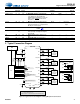
CS53L30 4 Functional Description 4 Functional Description This section provides a general description of the CS53L30 architecture and detailed functional descriptions of the various blocks that comprise the CS53L30. 4.1 Overview Fig. 4-1 is a block diagram of the CS53L30 with links to descriptions of major subblocks. VA See Section 4.4.
CS53L30 4.2 Resets The CS53L30 consists of the following blocks: • Interrupts. The CS53L30 QFN package includes an open-drain, active-low interrupt output, INT. Section 4.3 describes interrupts. • Capture-path inputs. The analog input block, described in Section 4.4, allows selection from either analog line-level, or analog mic sources. The selected analog source is fed into a mic preamplifier (when applicable) and then into a PGA, before entering the ADC.
CS53L30 4.4 Capture-Path Inputs 4.3.2 Interrupt Handling with the QFN Package The interrupt pin (INT) is implemented on the QFN package. Interrupt status bits can be individually masked by setting corresponding bits in the interrupt mask register (see Section 7.35). The configuration of mask bits determines which events cause the assertion of INT: • When an unmasked interrupt status event is detected, the status bit is set and INT is asserted.
CS53L30 4.4 Capture-Path Inputs Fig. 4-4 shows details of the various analog input gain settings, including control register fields. 0 or +20 dB and/or –96 to +12 dB with 1-dB steps or – dB (mute) –6 to +12 dB with 0.5-dB steps Bypass, +10, or +20 dB INx±, (x=1,2) PGA ADC1x_PREAMP on p. 54 ADC1x_PGA_VOL on p. 54 (Note 1) (Note 1) ADC1x ... Digital Gain Gain Adjust Adjust ADC1x_DIG_BOOST on p. 53 ADC1x_VOL on p. 54 Bypass, +10, or +20 dB INx±, (x=3,4) PGA ADC2x_PREAMP on p.
CS53L30 4.4 Capture-Path Inputs Board Chip 1.0 µF CINM Analog Differential Microphone CINM IN1+ VP IN1– MIC1_BIAS MIC_BIAS_FILT 4.7 µF GNDA Figure 4-6. Fully Differential Mic Input Connections Example Fig. 4-7 shows the IN1–IN4 interfaces and the related pseudodifferential connections recommended to achieve the best common-mode rejection for single-ended internal mics. Board Chip VP MIC1_BIAS 1.
CS53L30 4.5 Digital Microphone (DMIC) Interface 4.4.2 External Coupling Capacitors The analog inputs are internally biased to the internally generated common-mode voltage (VCM). Input signals must be AC coupled using external capacitors (CINM) with values consistent with the desired HPF design. The analog input resistance may be combined with an external capacitor to achieve the desired cutoff frequency. Eq. 4-1 provides an example for mic inputs.
CS53L30 4.5 Digital Microphone (DMIC) Interface 4.5.1 DMIC Interface Description The DMIC interface consists of a serial-data shift clock output (DMICx_SCLK) and a serial data input (DMICx_SD). Fig. 2-2 shows how to connect two digital mics (“Left” and “Right”) to the CS53L30. The clock is fanned out to both digital mics, and both digital mics’ data outputs share a single signal line to the CS53L30.
CS53L30 4.6 Serial Ports Table 4-1. Digital Mic Interface Clock Generation (Cont.) Post-MCLK_DIV MCLK Rate MCLK_INT_ ASP_RATE (MHz) SCALE (kHz) 1 6.1440 0 X 1 8, 11.025, 12 16, 22.050, 24 32, 44.1, 48 6.4000 0 X 1 8, 11.025, 12 16, 22.050, 24 32, 44.1, 48 Divide Ratio 2 4 2 4 2 4 2 4 2 4 2 4 2 4 2 4 DMICx_SCLK Rate DMICx_SCLK_DIV (MHz) Programming 3.0720 0 1.5360 1 0.7680 0 0.3840 1 1.5360 0 0.7680 1 3.0720 0 1.5360 1 3.2000 0 1.6000 1 0.8000 0 0.4000 1 1.6000 0 0.8000 1 3.2000 0 1.6000 1 1.
CS53L30 4.6 Serial Ports 4.6.3 High-Impedance Mode The serial port may be placed on a clock/data bus that allows multiple masters, without a need for external buffers. The ASP_3ST bit places the internal buffers for the serial port interface signals in a high-impedance state, allowing another device to transmit clocks and data without bus contention. If the CS53L30 serial port is a timing slave, its ASP_SCLK and ASP_LRCK/FSYNC I/Os are always inputs and are thus unaffected by the ASP_3ST control.
CS53L30 4.6 Serial Ports 4.6.5 Serial-Port Sample Rates Table 4-2 lists the supported sample rates. Before making changes to any clock setting or frequency, the device must be powered down by setting either the PDN_ULP or PDN_LP bit. v Table 4-2. Supported Master Clocks and Sample Rates MCLKEXT MCLKINT INTERNAL_FS_RATIO MCLK_INT_SCALE ASP_RATE (MHz) (MHz) Setting (MCLKINT/FSINT) MCLKINT Scaling 6.0000 6.
CS53L30 4.6 Serial Ports Table 4-2. Supported Master Clocks and Sample Rates (Cont.) MCLKEXT MCLKINT INTERNAL_FS_RATIO MCLK_INT_SCALE ASP_RATE (MHz) (MHz) Setting (MCLKINT/FSINT) MCLKINT Scaling 6.1440 6.1440 (MCLK_ 1 0 (disabled) 0001 DIV = 00) 1 (4) 0001 0 (disabled) 0010 1 (4) 0010 0 (disabled) 0100 1 (4) 0100 0 (disabled) 0101 1 (2) 0101 0 (disabled) 0110 1 (2) 0110 0 (disabled) 1000 1 (2) 1000 X 1001 X 1010 X 1100 1 0 (disabled) 0001 12.2880 6.
CS53L30 4.7 TDM Mode 1/Fsext LRCK Left (A) Channel Right (B) Channel SCLK may stop or continue SCLK ASP_SDOUTx MSB MSB-1 LSB+1 SCLK may stop or continue LSB MSB MSB-1 LSB+1 LSB textraA = None to some time Note: x = 1, 2 MSB textraB = None to some time Figure 4-11. I2S Format 4.6.6.1 I2S Format Bit Depths I2S interface data word length (see Section 4.6.6) is ambiguous.
CS53L30 4.7 TDM Mode FSYNC SCLK (ASP_SCLK_INV = 0, default) SDOUT (SHIFT_LEFT = 1) m:0 0:7 0:6 0:5 0:4 0:3 0:2 0:1 0:0 1:7 Slot 0 1:6 1:5 m:2 m:1 Slot 1 m:0 0:7 Slot m Figure 4-13. TDM Format—ASP_SCLK_INV = 0, SHIFT_LEFT = 1 FSYNC SCLK (ASP_SCLK_INV = 1) SDOUT (SHIFT_LEFT = 0, default) m:0 0:7 0:6 0:5 0:4 0:3 0:2 0:1 0:0 1:7 Slot 0 1:6 1:5 m:2 Slot 1 m:1 m:0 0:7 m:0 0:7 Slot m Figure 4-14.
CS53L30 4.7 TDM Mode Table 4-3. Slot Count and Resulting Unused Clock Cycles for Supported SCLK and Sample Rates (Cont.) SCLK Frequency [MHz] FSYNC Sample Rate [kHz] Number of Available Slots Resulting Number of Unused SCLK Cycles 6.0000 8.000 48 366 11.025 48 160 12.000 48 116 16.000 46 7 22.050 34 0 24.000 31 2 32.000 23 4 44.100 17 0 48.000 15 5 12.0000 8.000 48 1116 11.025 48 704 12.000 48 616 16.000 48 366 22.050 48 160 24.000 48 116 32.000 46 8 44.100 34 0 48.000 31 2 6.1440 8.000 48 384 11.
CS53L30 4.7 TDM Mode 4.7.3 Transmitting Data Fig. 4-17 shows the TDM transmit subblock. TDM Transmit Data Registers ASP _CH1 Data ASP _CHx Data ASP_SDOUT1 ASP _CH4 Data ASP _CH1_TX_LOC ASP _CHx_TX_LOC ASP _CH4_TX_LOC TDM Slot Assignment Control 48-bit TDM Slot Enable Control ASP_CH1_TX_STATE ASP _CHx_TX_STATE ASP_CH4_TX_STATE ASP _TX_ENABLE [47 :0 ] FSYNC SCLK Figure 4-17. TDM Transmit Subblock Diagram 4.7.3.
CS53L30 4.8 Synchronous Sample-Rate Converter (SRC) To maximize bus usage, the device supports hand-off between devices in a half clock cycle, which means no clock cycles have to be sacrificed during the hand-off between two devices. This behavior is shown in Table 3-12. If SHIFT_LEFT (see p. 45) is set, the hand-off between two devices has no margin and brief bus contention may occur.
CS53L30 4.9 Multichip Synchronization Protocol 4.9 Multichip Synchronization Protocol Due to the multidrop capability of the CS53L30 TDM bus, it is conceivable to employ up to four CS53L30 chips to allow up to 16 channels of audio capture. Extra care and sequencing steps have to be taken to ensure that the multichip configuration meets the channel-to-channel phase matching specification across chips when using multiple CS53L30 chips in a system.
CS53L30 4.12 MUTE Pin To use thermal overload notification, do the following: 1. Enable the thermal-sense circuitry by programming THMS_PDN (see p. 48). 2. Set M_THMS_TRIP (see p. 57) if an interrupt is desired when THMS_TRIP toggles from 0 to 1. 3. Monitor (read after interrupt [QFN only] or poll) the thermal overload interrupt status bit and respond accordingly. Except for the associated status bit, the operation of the CS53L30 is not affected by the thermal overload notification. 4.
CS53L30 4.14 I2C Control Port AD0 and AD1 are the logic state of the ASP_SDOUT2/AD0 and DMIC2_SCLK/AD1 pins, which are pulled to the supply or ground. These pins configure the I²C device address upon a device power up, after RESET is deasserted. These pins have internal pull-down resistors, allowing for the default I2C address with no external components. If an I2C address other than the default is desired, then external resistor termination to VA is required. The minimum resistor value allowed is 10 k.
CS53L30 4.
CS53L30 5.1 Octal Microphone Array to the Audio Serial Port 5.1 Octal Microphone Array to the Audio Serial Port Fig. 5-1 shows connections for an eight-channel mic array to serial port schematic configuration. MUTE MIC1_BIAS IN1+ IN1– MIC2_BIAS IN2+ IN2– MIC3_BIAS IN3+ IN3– MIC4_BIAS IN4+ IN4– ASP_SDOUT2/AD0 ASP_SDOUT1 ASP_SCLK CS53L30 ASP_LRCK MCLK RESET SDA Four-Channel Mic (see Connection Diagram) Four-Channel Mic Connection MIC1_BIAS IN1– SCL FILT+ VA GNDA +1.
CS53L30 5.2 Power-Up Sequence The CS53L30 includes a synchronization protocol that can be used to minimize channel-to-channel phase mismatch across multiple CS53L30s in a system, as long as the phase mismatch is not of the Class 1 type (i.e., deterministic, time invariant). An external phase calibration is necessary to nullify deterministic, time-invariant phase, which is beyond the scope of this document. The power-up sequence in Section 5.
CS53L30 5.2 Power-Up Sequence Example 5-1. Power-Up Sequence (Cont.) STEP TASK 6.4 Configure TDM channels. ASP TDM TX Control 1–4, Address 0x0E–0x11 ASP TDM TX Control 1, Address 0x0E ASP_CH1_STATE† Reserved ASP_CH1_TX_LOC[5:0]† ASP TDM TX Control 2, Address 0x0F ASP_CH2_STATE† Reserved ASP_CH2_TX_LOC[5:0]† ASP TDM TX Control 3, Address 0x10 ASP_CH3_STATE† Reserved ASP_CH3_TX_LOC[5:0]† ASP TDM TX Control 4, Address 0x11 ASP_CH4_STATE† Reserved ASP_CH4_TX_LOC[5:0]† 6.5 Enable TDM slots.
CS53L30 5.3 Power-Down Sequence Example 5-1. Power-Up Sequence (Cont.) STEP TASK 9.4 Configure the ADC2A ADC2A/2B AFE Control, Address 0x31–0x32 and ADC2B preamp ADC2A AFE Control, Address 0x31 and PGA settings. ADC2A_PREAMP[1:0]† ADC2A_PGA_VOL[5:0]† ADC2B AFE Control, Address 0x32 ADC2B_PREAMP[1:0]† ADC2B_PGA_VOL[5:0]† 0x40 01 ADC2A preamp gain is +10 dB. 00 0000 ADC2A PGA is set to 0 dB. 0x40 01 ADC2B preamp gain is +10 dB. 00 0000 ADC2B PGA is set to 0 dB. 9.
CS53L30 5.4 Capture-Path Inputs Example 5-2. Power-Down Sequence (Cont.) STEP TASK 3 Write the following registers to power down the device. REGISTER/BIT FIELDS VALUE DESCRIPTION Power Control, Address 0x06 PDN_ULP PDN_LP DISCHARGE_FILT+ THMS_PDN Reserved 0x90 1 0 0 1 0000 Ultralow power down is enabled. Power down is not enabled. FILT+ pin is not clamped to ground. Thermal sense is powered down. — 4 Poll the interrupt status register until the PDN_ DONE status bit is set.
CS53L30 5.4 Capture-Path Inputs VA +Vx GNDA IN+ –Vx GNDA 4Vx Vpp Differential signal VA +Vx GNDA IN– –Vx GNDA DC blocking capacitor Figure 5-2. Differential Analog Input Signal to IN±, with Protection Diodes Shown +Vx GNDA VA + 0.3 VA Vx + VA/2 To IN+ VA/2 –Vx + VA/2 GNDA GNDA – 0.3 4Vx Vpp Differential signal +Vx DC blocking capacitor –Vx GNDA VA + 0.3 VA Vx + VA/2 To IN– VA/2 –Vx + VA/2 GNDA GNDA – 0.3 –Vx Figure 5-3.
CS53L30 5.5 MCLK Jitter 5.5 MCLK Jitter The following analog and digital specifications listed in Section 3 are affected by MCLK jitter: • INx-to-x_SDOUT THD+N The effect of MCLK jitter on THD+N is due to sampling at an unintended time, resulting in sample error. The resulting sample error is a function of the time error as a result of MCLK jitter and of the slope of the signal being sampled or reconstructed.
CS53L30 6 Register Quick Reference 6 Register Quick Reference Default values are shown below the bit names. Adr. Function 7 6 5 4 0x00 Reserved 0 0x01 p. 47 0x02 p. 47 0x03 p. 47 0x04 Device ID A and B (Read Only) Device ID C and D (Read Only) Device ID E (Read Only) 0 0 0 1 1 0 0 0 0 0 MCLK_INT_ SCALE 0 — p. 50 0x10 ASP TDM TX Control 3 p.
CS53L30 6 Register Quick Reference Adr. Function 0x1B LRCK Control 1 p. 51 0x1C LRCK Control 2 p. 51 0x1D– Reserved 0x1E 7 6 5 4 3 2 1 0 LRCK_TPWH[10:3] 0 0 0 0 0 0 0 0 — LRCK_50_NPW LRCK_TPWH[2:0] 0 0 0 0 0 0 0 0 — 0 0 0 0 0 0 0 0 0x1F MUTE Pin Control 1 MUTE_PDN_ MUTE_PDN_LP — MUTE_M4B_ MUTE_M3B_ MUTE_M2B_ MUTE_M1B_ MUTE_MB_ ULP PDN PDN PDN PDN ALL_PDN p.
CS53L30 7 Register Descriptions 7 Register Descriptions All registers are read/write except for the chip ID, revision register, and status registers, which are read only. Refer to the following bit definition tables for bit assignment information. The default state of each bit after a power-up sequence or reset is indicated. All reserved registers must maintain their default state. 7.1 Device ID A and B R/O 7 Address 0x01 6 5 4 3 2 DEVIDA[3:0] Default 0 1 1 0 1 1 DEVIDB[3:0] 0 1 0 0 7.
CS53L30 7.6 MCLK Control Bits 5 Name Description DISCHARGE_ Discharge FILT+ capacitor. Configures the state of the FILT+ pin internal clamp. Before setting this bit, ensure that the FILT+ VA pin is connected to a supply, as described in Table 3-1. 0 (Default) FILT+ is not clamped to ground. 1 FILT+ is clamped to ground. This must be set only if PDN_ULP or PDN_LP = 1. Discharge time with an external 2.2-µF capacitor on FILT+ is ~46 ms. 4 THMS_PDN 3:0 — Thermal-sense power down.
CS53L30 7.8 Mic Bias Control 7.8 Mic Bias Control R/W 7 Address 0x0A 6 5 4 MIC4_BIAS_PDN MIC3_BIAS_PDN MIC2_BIAS_PDN MIC1_BIAS_PDN Default Bits 7, 6, 5, 4 Name MICx_ BIAS_ PDN 3 2 1:0 1 1 1 1 3 2 — VP_MIN 0 1 1 0 — VP_MIN VP supply minimum voltage setting. Configures the internal circuitry to accept the VP supply with the specified minimum value. These settings also affect PSRR; see Table 3-7. 0 3.0 V.
CS53L30 7.11 ASP TDM TX Control 1–4 7.11 ASP TDM TX Control 1–4 R/W 7 6 ASP_CHx_TX_STATE — 0 0 Default Bits 7 5 4 3 2 1 0 1 1 ASP_CHx_TX_LOC[5:0] 1 0 Name 1 1 Description ASP_ ASP TDM TX state control. Configures the state of the data for the ASP on Channel x. CHx_TX_ 0 (Default) Channel data is available STATE 1 Channel data is not available 6 5:0 Address 0x0E–0x11 — Reserved ASP_ ASP TDM TX location control.
CS53L30 7.15 LRCK Control 1 7.15 LRCK Control 1 R/W 7 Address 0x1B 6 5 4 3 2 1 0 0 0 0 LRCK_TPWH[10:3] Default Bits 7:0 0 0 0 0 Name 0 Description LRCK_ LRCK high-time pulse width [10:3]. With LRCK_TPWH[2:0], sets the number of SCLK cycles for which the LRCK remains TPWH[10:3] high. Active only when in TDM Mode and LRCK_50_NPW = 1. 0x000 (Default) LRCK high time is 1 SCLK wide 0x001 LRCK high time is 2 SCLKs wide 7.
CS53L30 7.19 Input Bias Control 1 Bits Name Description 4 MUTE_ASP_ SDOUT1_PDN Power down ASP_SDOUT1 when MUTE pin is asserted. Setting is ignored in TDM Mode. 0 (Default) Not affected by MUTE pin. 1 Powered down when MUTE pin asserted. 3, 2, MUTE_ADCxy_PDN Individual power down controls for the ADCs when the MUTE pin is asserted. 1, 0 0 (Default) Not affected by MUTE pin 1 Powered down when MUTE pin asserted 7.
CS53L30 7.24 ADC1/DMIC1 Control 2 Bits 1 Name Description DMIC1_ DMIC1 clock divide ratio. Selects the divide ratio between the internal MCLK and the digital mic interface clock output. SCLK_ Section 4.5 lists supported digital mic interface shift clock rates and their associated programming settings. DIV 0 (Default) 64•Fsint 1 32•Fsint 0 CH_ TYPE Input channel type. Sets the capture-path pins to be either all analog (analog mic/line-in) or all digital mic. 0 (Default) Analog inputs.
CS53L30 7.26 ADC1 Noise Gate Control 7.26 ADC1 Noise Gate Control R/W 7 6 5 ADC1B_NG ADC1A_NG ADC1_NG_BOOST 0 0 0 Default Bits Address 0x28 4 3 2 ADC1_NG_THRESH[2:0] 0 Name 1 0 ADC1_NG_DELAY[1:0] 0 0 0 0 Description 7,6 ADC1x_NG ADC1 noise gate enable for Channels A and B. Enables independent noise gating for Channels A and B if ADC1_NG_ ALL = 0. This bit has no effect if ADC1_NG_ALL = 1 0 (Default) Disable noise gating on Channel x 1 Enable noise gating on Channel x.
CS53L30 7.29 ADC2/DMIC2 Control 1 7.29 ADC2/DMIC2 Control 1 R/W 7 6 ADC2B_PDN ADC2A_PDN 0 0 Default Bits Address 0x2D 5 4 3 2 — 0 1 0 DMIC2_PDN DMIC2_SCLK_DIV 0 0 Name 1 — 0 0 Description 7,6 ADC2x_ ADC2x power down. Configures the ADC Channel x power state, including all associated analog front-end circuity (preamp, PDN PGA, etc.). Enables the channel’s digital decimator associated. Must be cleared if the input channel type is digital.
CS53L30 7.32 ADC2 Noise Gate Control 7.32 ADC2 Noise Gate Control R/W 7 6 5 ADC2B_NG ADC2A_NG ADC2_NG_BOOST 0 0 0 Default Bits Address 0x30 4 3 2 ADC2_NG_THRESH[2:0] 0 Name 1 0 ADC2_NG_DELAY[1:0] 0 0 0 0 Description 7,6 ADC2x_NG ADC2 noise-gate enable for Channels A and B. Enables independent noise gating for Channels A and B if ADC1_NG_ ALL = 0. This bit has no effect if ADC1_NG_ALL = 1 0 (Default) Disable noise gating on Channel x 1 Enable noise gating on Channel x.
CS53L30 7.35 Device Interrupt Mask 7.35 Device Interrupt Mask R/W 7 6 M_PDN_DONE M_THMS_TRIP Default Address 0x35 1 5 4 3 2 1 0 M_SYNC_ DONE M_ADC2B_ OVFL M_ADC2A_ OVFL M_ADC1B_ OVFL M_ADC1A_ OVFL M_MUTE_PIN 1 1 1 1 1 1 1 Interrupt mask register bits serve as a mask for the interrupt sources in the interrupt status registers. Interrupts are described in Section 4.3.
CS53L30 8 Parameter Definitions 8 Parameter Definitions Dynamic range. The ratio of the rms value of the signal to the rms sum of all other spectral components over the specified bandwidth. Dynamic range is a signal-to-noise ratio measurement over the specified band width made with a –60 dB signal. Frequency response. A measure of the amplitude response variation from 10 Hz to 20 kHz relative to the amplitude response at 1 kHz. Frequency response is expressed in decibel units. Gain drift.
CS53L30 9.1 Digital Filter Response 9.1.2 Combined ADC and SRC Response, Fsext = Fsint 0 0.25 -10 0.2 -20 0.15 -30 Magnitude (dB) Magnitude (dB) 0.1 0.05 0 -0.05 -40 -50 -60 -0.1 -70 -0.15 -80 -0.2 -90 -0.25 0 0.05 0.15 0.1 0.35 0.2 0.25 0.3 Frequency (Normalized to Fs) 0.4 0.45 -100 0.5 Figure 9-3. Passband—ADCx, Notch Enabled 0 1.5 2 1 Frequency (normalized to Fs) 0.5 2.5 3 Figure 9-4.
CS53L30 9.1 Digital Filter Response 0 0 -10 -100 -20 -30 Phase (degrees) Magnitude (dB) -200 -40 -50 -60 -300 -400 -70 -80 -500 -90 -100 0.3 0.35 0.4 0.55 0.45 0.5 Frequency (normalized to Fs) 0.6 0.65 -600 0.7 Figure 9-9. Transition Band—ADCx, Notch Disabled 9.1.3 0 0.05 0.1 0.15 0.3 0.2 0.25 Frequency (normalized to Fs) 0.35 0.4 0.45 0.5 Figure 9-10. Phase Response—ADCx, Notch Disabled Combined ADC and SRC Response, Fsext = 50 kHz, Fsint = 16 kHz, MCLK = 19.2 MHz 0 0.
CS53L30 9.1 Digital Filter Response 0 0.25 -20 0.2 0.15 -40 0.1 Magnitude (dB) Magnitude (dB) -60 0.05 0 -0.05 -80 -100 -0.1 -0.15 -120 -0.2 -140 -0.25 0 0.05 0.1 0.35 0.15 0.2 0.25 0.3 Frequency (normalized to Fs ext) 0.4 0.45 -160 0.5 Figure 9-15. Passband—ADCx, Notch Disabled 0 0.5 2.5 1 1.5 2 Frequency (normalized to Fs ext) 3 Figure 9-16.
CS53L30 9.2 PGA Gain Linearity 0 0 -10 -100 -20 -30 Phase (degrees) Magnitude (dB) -200 -40 -50 -60 -300 -400 -70 -80 -500 -90 -100 0.3 0.35 0.4 0.55 0.45 0.5 Frequency (normalized to Fs) 0.6 0.65 -600 0.7 Figure 9-21. Transition Band—DMICx, Notch Disabled 0 0.05 0.1 0.3 0.2 0.25 Frequency (normalized to Fs) 0.15 0.35 0.4 0.45 0.5 Figure 9-22. Phase Response—DMICx, Notch Disabled 9.2 PGA Gain Linearity 0.525 12.0 0.520 10.0 0.515 8.0 0.
CS53L30 9.3 Dynamic Range Versus Sampling Frequency 9.3 Dynamic Range Versus Sampling Frequency 100 99 MCLK_INT_SCALE = 0 Dynamic Range (dB, AͲweighted) 98 97 96 95 94 93 MCLK_INT_SCALE = 1 92 91 90 8 kHz 11.025 kHz 12 kHz 16 kHz 22.05 kHz 24 kHz 32 kHz 44.1 kHz 48 kHz Sampling Frequency (Fsext) Figure 9-25. Dynamic Range Versus Sampling Frequency 9.
CS53L30 9.4 FFTs G % ) 6 G % ) 6 N N N N N G % ) 6 N N N N N Figure 9-29. FFT, 1 kHz, –1 dBFS, Preamp Setting: +10 dB, PGA Setting: +12 dB, Fsint = Fsext = 48 kHz Figure 9-28.
CS53L30 10 Package Dimensions 10 Package Dimensions 10.1 WLCSP Package Ball A1 location indicator (seen through package) M A A2 X X A1 Ball A1 Location Indicator Ball A1 Z Y N e X WAFER BACK SIDE b øb Øddd Z X Y Øccc Z Seating plane e SIDE VIEW d c BUMP SIDE Notes: • Dimensioning and tolerances per ASME Y 14.5M–1994. • The Ball A1 position indicator is for illustration purposes only and may not be to scale.
CS53L30 10.2 QFN Package 10.2 QFN Package b D e Pin #1 Corner Pin #1 Corner E E2 A1 A Top View L D2 Side View Bottom View Figure 10-2. 32-Pin QFN Package Drawing 1 Dim Millimeters Nom Min A A1 b D D2 E E2 e L — 0.00 0.20 — — 0.25 5.00 BSC 3.65 5.00 BSC 3.65 0.50 BSC 0.40 3.55 3.55 0.35 Max 1.00 0.05 0.30 3.75 3.75 0.45 JEDEC #: MO–220 Controlling dimension is millimeters. 1. Dimensioning and tolerances per ASME Y 14.5M–1995. 2.
CS53L30 13 Revision History 13 Revision History Revision F1 Change Provided specific range of audio sample rates in System Features section on p. 1. Added Note 6 to Fig. 2-1 and Fig. 2-2. Added reference to Section 5.7 in Note 8 in Fig. 2-2. Updated mic bias startup delay specification in Table 3-6. Added power consumption register field settings in Table 3-9. Updated maximum SCLK duty cycle specification for I2S master mode in Table 3-11.