
Manual


CS5378
DS639F3 58
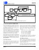
16.SERIAL DATA INTERFACE
Once digital filtering is complete, each 24-bit out-
put sample is combined with an 8-bit status byte.
These data words are written to an 8-deep FIFO
buffer and then transmitted to the communications
channel through a high speed serial data interface.
16.1 Pin Descriptions
DRDY
- Pin 23
Data ready output signal, active low. Open drain
output requiring an external pull-up resistor.
SCK - Pin 24
Serial clock input.
MISO - Pin 25
Serial data output.
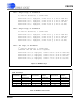
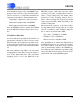
16.2 Serial Data Format
Serial data transactions transfer either 24-bit data
words or 32-bit status+data words, depending on
the STAT bit in the CONFIG register. When trans-
mitting status information, each 8-bit status byte
has an MFLAG bit, a time break bit, and a FIFO
overflow bit encoded as shown in Figure 34.
MFLAG Bit - MFLAG
The MFLAG bit is set in the status byte when an
signal is received on the MFLAG pin. When re-
CS5378
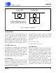
Figure 33. Serial Data Interface Block Diagram
System Telemetry
MISO
DRDY
SCK
Data Ready
Data In
Clock Out
Data
Status
02331
--
MFLAG
-- --
W
31 2930 28 27 26 25 24
Figure 34. 32-bit Serial Data Format
TB
--
--
0 - Modulator Ok
1 - Modulator Error
0 - No Time Break
1 - Time Break
0 - FIFO Ok
1 - FIFO Overflow