
Manual


CS5378
DS639F3 13
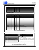
THERMAL CHARACTERISTICS
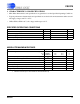
DIGITAL CHARACTERISTICS
Notes: 2. Maximum leakage for pins with pull-up resistors (RESET, SS:EECS, GPIO, MOSI, SCK) is ±250 μA.
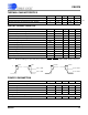
POWER CONSUMPTION
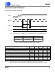
Parameter Symbol Min Typ Max Unit
Allowable Junction Temperature T
J
--135°C
Junction to Ambient Thermal Impedance (4-Layer PCB) Θ
JA
-50 °C / W
Ambient Operating Temperature (Power Applied) T
A
-40 - +85 °C
Parameter Symbol Min Typ Max Unit
High-Level Input Drive Voltage V
IH
0.6 * VDD - VDD V
Low-Level Input Drive Voltage V
IL
0.0 - 0.8 V
High-Level Output Drive Voltage I
out
= -40 µA V
OH
VDD - 0.3 - VDD V
Low-Level Output Drive Voltage I
out
= +40 µA V
OL
0.0 - 0.3 V
Rise Times, Digital Inputs t
RISE
--100ns
Fall Times, Digital Inputs t
FALL
--100ns
Rise Times, Digital Outputs t
RISE
--100ns
Fall Times, Digital Outputs t
FALL
--100ns
Input Leakage Current (Note 2) I
IN
-± 1± 10µA
3-State Leakage Current I
OZ
--± 10µA
Digital Input Capacitance C
IN
-9-pF
Digital Output Pin Capacitance C
OUT
-9-pF
Parameter Symbol Min Typ Max Unit
Operational Power Consumption
1.024 MHz Digital Filter Clock PWR
1
-12-mW
2.048 MHz Digital Filter Clock PWR
2
-14-mW
4.096 MHz Digital Filter Clock PWR
4
-16-mW
8.192 MHz Digital Filter Clock PWR
8
-24-mW
Standby Power Consumption
32 kHz Digital Filter Clock, Filter Stopped PWR
S
- 100 - µW
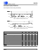
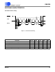
2.6 V
0.7 V
t
fallin
t
risein
4.6 V
0.4 V
t
riseout
t
fallout
0.90 * VDD
0.10 * VDD
0.90 * VDD
0.10 * VDD