CS5378 Low-power Single-channel Decimation Filter Features Description Single-channel Digital Decimation Filter Multiple On-chip FIR and IIR Coefficient Sets Programmable Coefficients for Custom Filters Synchronous Operation Integrated PLL for Clock Generation 1.024 MHz, 2.048 MHz, or 4.
CS5378 TABLE OF CONTENTS 1. General Description . . . . . . . . . . . . . . . . . . . . . . . . . . . . . . . . . . . . . . 6 1.1. 1.2. 1.3. 1.4. Digital Filter Features . . . . . . . . . . . . . . . . . . . . . . . . . . . . . . . . . . . . . . . .6 Integrated Peripheral Features . . . . . . . . . . . . . . . . . . . . . . . . . . . . . . . .7 System Level Features . . . . . . . . . . . . . . . . . . . . . . . . . . . . . . . . . . . . . .7 Configuration Interface. . . . . . . . . . . . . . . . . . . . .
CS5378 9.1. 9.2. 9.3. 9.4. 9.5. Pin Descriptions . . . . . . . . . . . . . . . . . . . . . . . . . . . . . . . . . . . . . . . . . . .30 Microcontroller Hardware Interface . . . . . . . . . . . . . . . . . . . . . . . . . . . .30 Microcontroller Serial Transactions . . . . . . . . . . . . . . . . . . . . . . . . . . . .30 Microcontroller Configuration Commands . . . . . . . . . . . . . . . . . . . . . . .33 Example Microcontroller Configuration . . . . . . . . . . . . . . . . . . . . . . . . .35 10.
CS5378 17.7. TBS Synchronization . . . . . . . . . . . . . . . . . . . . . . . . . . . . . . . . . . . . . .62 18. Time Break Controller . . . . . . . . . . . . . . . . . . . . . . . . . . . . . . . . . . . 63 18.1. Pin Description . . . . . . . . . . . . . . . . . . . . . . . . . . . . . . . . . . . . . . . . . . .63 18.2. Time Break Operation . . . . . . . . . . . . . . . . . . . . . . . . . . . . . . . . . . . . .63 18.3. Time Break Delay. . . . . . . . . . . . . . . . . . . . . . . . . . . . . . . . .
CS5378 Figure 29. Figure 30. Figure 31. Figure 32. Figure 33. Figure 34. Figure 35. Figure 36. Figure 37. Figure 38. Figure 39. Figure 40. Figure 41. Figure 42. Figure 43. Figure 44. Figure 45. Figure 46. Figure 47. Figure 48. Figure 49. Figure 50. Figure 51. Figure 52. Figure 53. Figure 54. FIR2 Minimum Phase Coefficients . . . . . . . . . . . . . . . . . . . . . . . . . . . . . . . . IIR Filter Block Diagram . . . . . . . . . . . . . . . . . . . . . . . . . . . . . . . . . . . . . . . .
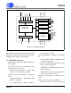
VDDCORE VDDPLL VDDPAD DRDY MISO MOSI SCK SS:EECS CS5378 PLL, Clock Generation CLK MCLK Reset, Synchronization RESET SYNC MSYNC Time Break Controller TIMEB Serial Interface Decimation and Filtering Engine Test Bit Stream Controller GPIO7:BOOT GPIO6:PLL2 GPIO5:PLL1 GPIO4:PLL0 GPIO3 GPIO2 GPIO1 GPIO0 GNDCORE GNDPAD MFLAG MDATA GNDPLL GPIO General Purpose I/O Modulator Data Interface TBSDATA Figure 1. CS5378 Block Diagram 1.
CS5378 Modulator Input 512 kHz Sinc Filter 2 - 64000 FIR1 FIR2 4 Gain & DC Offset Corrections IIR1 st 2 1 Order IIR2 2 nd Order Output to High Speed Serial Interface Output Word Rate from 4000 SPS ~ 1 SPS Figure 2. Digital Filtering Stages DC offset. - • Calibration engine for automatic calculation of offset correction factor. 1.2 Integrated Peripheral Features • • Dedicated TB status bit in the output data stream. - Programmable output delay to match system group delay. 1.024 MHz, 2.
CS5378 - from 3.3 V or 5 V. • Digital logic core operates from 2.5 V, 3.3 V or 5 V. Small 28-pin SSOP package. Configuration commands written through the serial interface. (See Table 1) - - Standardized microcontroller interface using SPI™ registers. (See Table 3) - Commands write digital filter registers and FIR / IIR filter coefficients. - Digital filter registers set hardware configuration options. Total footprint 8 mm x 10 mm plus three bypass capacitors. • 1.
CS5378 Microcontroller Boot Configuration Commands Name CMD 24-bit DAT1 24-bit DAT2 24-bit Description NOP 000000 - - WRITE DF REGISTER 000001 REG DATA Write Digital Filter Register READ DF REGISTER 000002 REG [DATA] - Read Digital Filter Register WRITE FIR COEFFICIENTS 000003 NUM FIR1 (FIR COEF) NUM FIR2 (FIR COEF) Write Custom FIR Coefficients WRITE IIR COEFFICIENTS 000004 a11 b11 a22 b21 b10 a21 b20 b22 Write Custom IIR Coefficients WRITE ROM COEFFICIENTS 000005 COEF SEL -
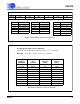
CS5378 Bits 23:20 19:16 15:12 11:8 7:4 3:0 Selection 0000 0000 IIR2 IIR1 FIR2 FIR1 Bits 15:12 IIR2 Coefficients Bits 11:8 IIR1 Coefficients Bits 3:0 FIR1 Coefficients 0000 3 Hz @ 2000 SPS 0000 3 Hz @ 2000 SPS 0000 Linear Phase 0001 3 Hz @ 1000 SPS 0001 3 Hz @ 1000 SPS 0001 Minimum Phase 0010 3 Hz @ 500 SPS 0010 3 Hz @ 500 SPS 0011 3 Hz @ 333 SPS 0011 3 Hz @ 333 SPS Bits 7:4 FIR2 Coefficients 0100 3 Hz @ 250 SPS 0100 3 Hz @ 250 SPS 0000 Linear Phase 0001 Mini
CS5378 SPI Registers Addr. Type # Bits SPICTRL Name 00 - 02 R/W 8, 8, 8 SPI Control Description SPICMD 03 - 05 R/W 8, 8, 8 SPI Command SPIDAT1 06 - 08 R/W 8, 8, 8 SPI Data 1 SPIDAT2 09 - 0B R/W 8, 8, 8 SPI Data 2 Addr.
CS5378 2. CHARACTERISTICS AND SPECIFICATIONS • Min / Max characteristics and specifications are guaranteed over the Specified Operating Conditions. • Typical performance characteristics and specifications are derived from measurements taken at nominal supply voltages and TA = 25°C. • GND, GND1, GND2 = 0 V, all voltages with respect to 0 V. SPECIFIED OPERATING CONDITIONS Parameter Logic Core Power Supply Symbol Min Nom Max Unit VDDCORE 2.375 2.5 5.25 V VDDPLL 3.135 3.3 5.25 V VDDPAD 3.
CS5378 THERMAL CHARACTERISTICS Parameter Allowable Junction Temperature Junction to Ambient Thermal Impedance (4-Layer PCB) Ambient Operating Temperature (Power Applied) Symbol Min Typ Max Unit TJ - - 135 °C - 50 -40 - Symbol Min Typ Max Unit VIH 0.6 * VDD - VDD V 0.0 - 0.8 V ΘJA TA °C +85 /W °C DIGITAL CHARACTERISTICS Parameter High-Level Input Drive Voltage Low-Level Input Drive Voltage VIL High-Level Output Drive Voltage Iout = -40 µA VOH VDD - 0.
CS5378 SWITCHING CHARACTERISTICS Serial Configuration Interface Timing (External Master) SSI SS:EECS MOSI MSB LSB MSB - 1 t1 t2 t3 t4 t5 t6 SCK SCLK Figure 4. MOSI Write Timing in SPI Slave Mode SS I SS:EECS t 10 MISO MSB MSB - 1 t7 SCK SCLK LSB t8 t9 Figure 5.
CS5378 SWITCHING CHARACTERISTICS Serial Data Interface Timing DRDY SCK t3 t4 MISO t1 t2 t5 Figure 6.
CS5378 SWITCHING CHARACTERISTICS CLK, SYNC, MCLK, MSYNC, and MDATA SYNC MCLK MSYNC tmsd tmsh tmsd Data1 MDATA Data2 Note: SYNC input latched on MCLK rising edge. MSYNC output triggered by MCLK falling edge. fMCLK 2.048 MHz 1.024 MHz tmsd = TMCLK / 4 tmsd = 122 ns tmsd = 244 ns tmsh = TMCLK tmsh = 488 ns tmsh = 976 ns Figure 7. SYNC, MCLK, MSYNC, MDATA Interface Timing Parameter Symbol Min Typ Max Unit CLK 32 32.
CS5378 SWITCHING CHARACTERISTICS Test Bit Stream (TBS) TBSDATA t1 t2 MCLK Note: Example timing shown for a 256 kHz output rate and no programmable delays. Figure 8. TBS Output Data Timing Parameter Symbol Min Typ Max Unit - 256 - kbps t1 60 - - ns t2 60 - - ns TBS Data Output Timing TBS Data Bit Rate TBS Data Rising to MCLK Rising Setup Time MCLK Rising to TBS Data Falling Hold Time (Note 5) 5. TBSDATA can be delayed from 0 to 63 full bit periods.
CS5378 CS5373A Differential Sensor M U X CS3301A CS3302A AMP CS5378 ΔΣ Modulator μController or Configuration EEPROM Digital Filter System Telemetry Test DAC Figure 9. Single-Channel System Block Diagram 3. SYSTEM DESIGN WITH CS5378 Figure 9 illustrates a simplified block diagram of the CS5378 in a single channel measurement system. A differential sensor is connected through the CS3301A/02A differential amplifiers to the CS5373A ΔΣ modulator, where analog to digital conversion occurs.
CS5378 3.4 Synchronization 3.7 Data Collection Digital filter phase and analog sample timing of the ΔΣ modulator connected to the CS5378 are synchronized by a rising edge on the SYNC pin. If a synchronization signal is received identically by all CS5378 devices in a measurement network, synchronous sampling across the network is guaranteed. Data is collected from the CS5378 through the serial data interface.
CS5378 VDDPAD GNDPAD 1 28 2 27 3 26 4 25 5 24 6 23 7 22 8 21 9 20 10 19 11 18 12 17 13 16 14 15 GNDCORE VDDCORE GNDPLL VDDPLL Figure 10. Power Supply Block Diagram 4. POWER SUPPLIES The CS5378 has three sets of power supply inputs. One set supplies power to the I/O pins of the device (VDDPAD), another supplies power to the logic core (VDDCORE) and the third supplies power to the PLL (VDDPLL).
CS5378 RESET Self-Tests BOOT Pin 0 1 SELFTEST Register EEPROM Boot μController Boot Figure 11. Reset Control Block Diagram 5. RESET CONTROL The CS5378 reset signal is active low. When released, a series of self-tests are performed and the device either actively boots from an external EEPROM or enters an idle state waiting for microcontroller configuration. combined into the SELFTEST register (0x2F), with 0x0AAAAA indicating all passed. Self-tests require 60 ms to complete. 5.
CS5378 CLK PLL 32.768 MHz Internal Clocks Clock Divider and MCLK Generator PLL[2:0] MCLK Output DSPCFG Register Figure 12. Clock Generation Block Diagram 6. PLL AND CLOCK GENERATION The CS5378 requires a 32.768 MHz master clock, which can be supplied directly or from an internal phase locked loop. This master clock is used to generate an internal digital filter clock and an external modulator clock. The internal PLL will lock to standard clock or Manchester encoded input signals.
CS5378 6.4 Master Clock Jitter and Skew Care must be taken to minimize jitter and skew on the distributed system clock as both parameters affect measurement performance. DS639F3 Jitter on the input clock causes jitter in the generated modulator clock, resulting in sample timing errors and increased noise. Skew between input clocks from node to node creates a sample timing offset, resulting in systematic measurement errors in a reconstructed signal.
CS5378 0 SYNC 1 MSYNC Generator Digital Filter 0 1 MSYNC Output MSEN Test Bit Stream TSYNC Figure 13. Synchronization Block Diagram 7. SYNCHRONIZATION The CS5378 has a dedicated SYNC input that aligns the internal digital filter phase and generates an external signal for synchronizing modulator analog sampling. By providing simultaneous rising edges to the SYNC pins of multiple CS5378 devices, synchronous sampling across a network can be guaranteed. phase.
CS5378 VD SS:EECS SCK CS5378 MISO MOSI 27 1 24 6 25 2 26 5 CS 3 8 7 WP VCC HOLD SCK AT25640 SO SI 4 GND Figure 14. EEPROM Configuration Block Diagram 8. CONFIGURATION BY EEPROM After reset, the CS5378 reads the state of the GPIO7:BOOT pin to determine a source for configuration commands. If BOOT is high, the CS5378 initiates serial transactions to read configuration information from an external EEPROM. 8.
CS5378 Instruction Read Opcode Address 0x03 Definition ADDR[15:0] Read data beginning at the address given in ADDR. Serial Read from EEPROM 2 BYTE ADDR READ CMD 0x03 MOSI ADDR ADDR DATA1 DATA2 DATA3 MISO 1 BYTE / 3 BYTE DATA SS:EECS Cycle 1 2 3 4 5 6 7 8 MSB 6 5 4 3 2 1 LSB 6 5 4 3 2 1 LSB SCK MOSI MISO MSB X SS:EECS Figure 15.
CS5378 Write DF Register - 0x01 0000h 0010h Mfg Header 8-bit Command N x 24-bit Data 8-bit Command N x 24-bit Data 1FFFh EEPROM Manufacturing Information EEPROM Command and Data Values This EEPROM command writes a data value to the specified digital filter register. Digital filter registers control hardware peripherals and filtering functions. See “Digital Filter Registers” on page 71 for the bit definitions of the digital filter registers.
CS5378 Sample Command: Sample Command: Write IIR1 coefficients 0x84BC9D, 0x7DA1B1, 0x825E4F, and IIR2 coefficients 0x83694F, 0x3CAD5F, 0x3E5104, 0x835DF8, 0x3E5104. Select IIR1 and IIR2 3 Hz @ 500 SPS low-cut coefficients, with FIR1 and FIR2 linear phase highcut coefficients. Data word 0x002200. 03 04 00 22 00 84 BC 9D 7D A1 B1 82 5E 4F 83 69 4F Filter Start - 0x07 3C AD 5F 3E 51 04 83 5D F8 3E 51 04 This EEPROM command initializes and starts the digital filter.
CS5378 8.5 Example EEPROM Configuration Table 8 shows an example EEPROM file for a minimal CS5378 configuration.
CS5378 Digital Filter Command Interpreter SPI™ Registers Serial Pin Logic SS:EECS SCK MOSI MISO Figure 17. Serial Interface Block Diagram 9. CONFIGURATION BY MICROCONTROLLER After reset, the CS5378 reads the state of the GPIO7:BOOT pin to determine a source for configuration commands. If BOOT is low, the CS5378 receives configuration commands from a microcontroller. 9.1 Pin Descriptions Pins required for microcontroller boot are listed here, other serial pins are inactive.
CS5378 Instruction Opcode Address Definition Write 0x02 ADDR[7:0] Write SPI registers beginning at the address in ADDR. Read 0x03 ADDR[7:0] Read SPI registers beginning at the address in ADDR.
CS5378 9.3.2 SPI registers The SPI registers are shown in Figure 19 and are 24-bit registers mapped into an 8-bit register space as high, mid, and low bytes. See “SPI Registers” on page 66 for the bit definitions of the SPI registers. MOSI: 03 01 00 MISO: xx xx 12 5-byte read of SPIDAT1 MOSI: 03 06 00 00 00 MISO: xx xx 12 34 56 9.3.
CS5378 9.4 Microcontroller Configuration Commands Read DF Register - 0x02 A summary of available microcontroller configuration commands is listed in Table 9. Write DF Register - 0x01 This configuration command writes a specified digital filter register. Digital filter registers control hardware peripherals and filtering functions. See “Digital Filter Registers” on page 71 for the bit definitions of the digital filter registers. This command reads a specified digital filter register.
CS5378 Write FIR Coefficients - 0x03 02 06 3C AD 5F 3E 51 04 This command writes custom coefficients for the FIR1 and FIR2 filters. The first two data words set the number of FIR1 and FIR2 coefficients to be written. The remaining data words are the concatenated FIR1 and FIR2 coefficients. Delay 1 ms or poll E2DREQ A maximum of 255 coefficients can be written for each FIR filter, though the available digital filter computation cycles will limit their practical size.
CS5378 9.5 Example Microcontroller Configuration Table 10 shows an example microcontroller transactions for a minimal CS5378 configuration.
CS5378 MCLK MSYNC MCLK / MSYNC Generate MDATA MDI Input MFLAG 512 kHz CLK SYNC SINC Filter DC Offset & Gain Correction FIR Filters IIR Filter Output to High Speed Serial Interface Output Rate 4000 SPS ~ 1 SPS Figure 20. Modulator Data Interface 10. MODULATOR INTERFACE The CS5378 performs digital filtering for a ΔΣ type modulator. Signals from the ΔΣ modulators are connected through the modulator data interface (MDI). 10.2 Modulator Clock Generation 10.
CS5378 10.4 Modulator Data Input 10.5 Modulator Flag Input The MDATA input expects 1-bit ΔΣ data at a 512 kHz or 256 kHz rate. The input rate is selected by a bit in the CONFIG register (0x00). By default, MDATA is expected at 512 kHz. A high MFLAG input signal indicates the ΔΣ modulator has become unstable due to an analog overrange input signal. Once the over-range signal is reduced, the modulator recovers stability and the MFLAG signal is cleared.
CS5378 Modulator Input 512 kHz SINC Filter FIR1 2 - 64000 DC Offset & Gain Correction 4 FIR2 IIR1 2 1st Order IIR2 2nd Order Output to High Speed Serial Data Interface Output Rate 4000 SPS ~ 1 SPS Figure 21. Digital Filter Stages 11. DIGITAL FILTER INITIALIZATION The CS5378 digital filter consists of three multistage sections: a three stage SINC filter, a two stage FIR filter, and a two stage IIR filter.
CS5378 Bits 23:20 19:16 15:12 11:8 7:4 3:0 Selection 0000 0000 IIR2 IIR1 FIR2 FIR1 Bits 15:12 IIR2 Coefficients Bits 11:8 IIR1 Coefficients Bits 3:0 FIR1 Coefficients 0000 3 Hz @ 2000 SPS 0000 3 Hz @ 2000 SPS 0000 Linear Phase 0001 3 Hz @ 1000 SPS 0001 3 Hz @ 1000 SPS 0001 Minimum Phase 0010 3 Hz @ 500 SPS 0010 3 Hz @ 500 SPS 0011 3 Hz @ 333 SPS 0011 3 Hz @ 333 SPS Bits 7:4 FIR2 Coefficients 0100 3 Hz @ 250 SPS 0100 3 Hz @ 250 SPS 0000 Linear Phase 0001 Mini
CS5378 1-bit Δ−Σ Input 4th order sinc3 stage1 5 5th order sinc1 8 4th order sinc3 stage2 5 4th order sinc2 stage1 2 4th order sinc3 stage3 5 4th order sinc2 stage2 2 5th order sinc3 stage4 5 5th order sinc2 stage3 2 5th order sinc3 stage5 2 6th order sinc2 stage4 2 6th order sinc3 stage6 3 6th order sinc3 stage7 2 24-bit Output Figure 23. SINC Filter Block Diagram 12. SINC FILTER The SINC filter primary purpose is to attenuate outof-band noise components from the ΔΣ modulators.
CS5378 SINC1 – Single stage, fixed decimate by 8 5th order decimate by 8, 36 coefficients SINC2 – Multi-stage, variable decimation Stage Stage Stage Stage 1: 2: 3: 4: 4th 4th 5th 6th order order order order decimate decimate decimate decimate by by by by 2, 2, 2, 2, 5 5 6 7 coefficients coefficients coefficients coefficients SINC3 – Multi-stage, variable decimation Stage Stage Stage Stage Stage Stage Stage 1: 2: 3: 4: 5: 6: 7: 4th 4th 4th 5th 5th 6th 6th order order order order order order orde
CS5378 Filter Type System Function SINC1 5th order decimate by 8 36 coefficients 1 − z −8 H ( z ) = −1 1− z Filter Type System Function SINC2 (Stage 1) SINC2 (Stage 2) 4th order decimate by 2 5 coefficients 1 − z −2 H ( z ) = −1 1− z 4 h0 h1 h2 h3 h4 = = = = = 1 4 6 4 1 SINC2 (Stage 3) 5th order decimate by 2 6 coefficients 1 − z −2 H ( z ) = −1 1− z 5 h0 h1 h2 h3 h4 h5 = = = = = = 1 5 10 10 5 1 SINC2 (Stage 4) 6th order decimate by 2 7 coefficien
CS5378 Filter Type System Function Filter Coefficients SINC3 (Stage 1) SINC3 (Stage 2) SINC3 (Stage 3) 4th order decimate by 5 17 coefficients 1 − z −5 H ( z ) = −1 1− z 4 h0 h1 h2 h3 h4 h5 h6 h7 h8 SINC3 (Stage 4) 5th order decimate by 5 21 coefficients 1 − z −5 H ( z ) = −1 1 z − 5 h0 = 1 h1 = 5 h2 = 15 h3 = 35 h4 = 70 h5 = 121 h6 = 185 h7 = 255 h8 = 320 h9 = 365 h10 = 381 SINC3 (Stage 5) 5th order decimate by 2 6 coefficients 1 − z −2 H ( z ) = −1 1 −
CS5378 FIR1 Filter - decimate by 4 FIR2 Filter - decimate by 2 Figure 25. FIR Filter Block Diagram 13. FIR FILTER The finite impulse response (FIR) filter block consists of two cascaded stages, FIR1 and FIR2. It compensates for SINC filter droop and creates a low-pass corner to block aliased components of the input signal. On-chip linear phase or minimum phase coefficients can be selected using a configuration command, or the coefficients can be programmed for a custom filter response. 13.
CS5378 13.3 On-Chip FIR Coefficients Two sets of on-chip coefficients, linear phase and minimum phase, are available for FIR1 and FIR2. Performance of the on-chip coefficient sets is very good, with excellent ripple and stop band characteristics as described in Figure 26 and Table 14. scale, 0x7FFFFF, and scale all other coefficients accordingly.
CS5378 FIR1 – Single stage, fixed decimate by 4 Coefficient set 0: linear phase decimate by 4, 48 coefficients Coefficient set 1: minimum phase decimate by 4, 48 coefficients SINC droop compensation filter FIR2 – Single stage, fixed decimate by 2 Coefficient set 0: linear phase decimate by 2, 126 coefficients Coefficient set 1: minimum phase decimate by 2, 126 coefficients Brick wall low-pass filter, flat to 40% fs Combined SINC + FIR digital filter specifications Passband ripple less than +/- 0.
CS5378 Individual filter stage group delay (no IIR) Decimation Ratios 8 SINC1 SINC2 Stage 4 Stages 3,4 Stages 2,3,4 Stages 1,2,3,4 Number of Coefficients 36 Group Delay (Input Rate) 17.5 2 2,2 2,2,2 2,2,2,2 7 6,7 5,6,7 5,5,6,7 3.0 8.5 19.0 40.0 2 3 2,2 5,2 5,2,2 5,5,2 5,5,2,2 5,5,5,2,2 7 13 6,7 21,7 17,6,7 17,21,7 17,17,6,7 17,17,17,6,7 3.0 6.0 8.5 25.0 50.5 133.0 260.5 1310.5 Coefficient Set 0 Coefficient Set 1 4 4 48 48 23.5 See Figure Coefficient Set 0 Coefficient Set 1 2 2 126 126 62.
CS5378 Minimum phase group delay FIR1 Minimum Phase Group Delay (Normalized frequency) FIR2 Minimum Phase Group Delay (Normalized frequency) Table 16.
CS5378 Filter Type FIR1 (Coefficient set 0) Low pass, SINC compensation Linear phase decimate by 4 48 coefficients FIR1 (Coefficient set 1) Low pass, SINC compensation Minimum phase decimate by 4 48 coefficients Filter Coefficients (normalized 24-bit) h0 = 558 h24 h1 = 1905 h25 h2 = 3834 h26 h3 = 5118 h27 h4 = 365 h28 h5 = -14518 h29 h6 = -39787 h30 h7 = -67365 h31 h8 = -69909 h32 h9 = -19450 h33 h10 = 97434 h34 h11 = 258881 h35 h12 = 375562 h36 h13 = 332367 h37 h14 = 39864 h38 h15 = -496361 h39 h16 = -10
CS5378 Filter Type Filter Coefficients (normalized 24-bit) FIR2 (Coefficient set 0) Low pass, passband to 40% fs Linear phase decimate by 2 126 coefficients h0 h1 h2 h3 h4 h5 h6 h7 h8 h9 h10 h11 h12 h13 h14 h15 h16 h17 h18 h19 h20 h21 h22 h23 h24 h25 h26 h27 h28 h29 h30 h31 h32 h33 h34 h35 h36 h37 h38 h39 h40 h41 h42 h43 h44 h45 h46 h47 h48 h49 h50 h51 h52 h53 h54 h55 h56 h57 h58 h59 h60 h61 h62 = = = = = = = = = = = = = = = = = = = = = = = = = = = = = = = = = = = = = = = = = = = = = = = = = = = = = = =
CS5378 Filter Type Filter Coefficients (normalized 24-bit) FIR2 (Coefficient set 1) Low pass, passband to 40% fs Minimum phase decimate by 2 126 coefficients h0 h1 h2 h3 h4 h5 h6 h7 h8 h9 h10 h11 h12 h13 h14 h15 h16 h17 h18 h19 h20 h21 h22 h23 h24 h25 h26 h27 h28 h29 h30 h31 h32 h33 h34 h35 h36 h37 h38 h39 h40 h41 h42 h43 h44 h45 h46 h47 h48 h49 h50 h51 h52 h53 h54 h55 h56 h57 h58 h59 h60 h61 h62 = = = = = = = = = = = = = = = = = = = = = = = = = = = = = = = = = = = = = = = = = = = = = = = = = = = = = =
CS5378 1st Order IIR1 2nd Order IIR2 b10 b20 Z-1 Z-1 -a11 b11 -a21 b21 Z-1 3rd Order IIR3 implemented by running both IIR1 and IIR2 stages -a22 b22 Figure 30. IIR Filter Block Diagram 14. IIR FILTER The infinite impulse response (IIR) filter block consists of two cascaded stages, IIR1 and IIR2. It creates a high-pass corner to block very low-frequency and DC components of the input signal.
CS5378 characteristic equations model the operation of the 2nd order IIR filter with unnormalized coefficients. W5 = W4 W4 = W3 Which on-chip coefficient set to use is selected by a data word following the ‘Write ROM Coefficients’ configuration command. See “Filter Coefficient Selection” on page 38 for information about selecting on-chip coefficient sets. W3 = X + (-a21 * W4) + (-a22 * W5) Y = (W3 * b20) + (W4 * b21) + (W5 * b22) 14.
CS5378 IIR1 – Single stage, no decimation 1st order no decimation, 3 coefficients Coefficient Coefficient Coefficient Coefficient Coefficient set set set set set 0: 1: 2: 3: 4: high-pass, high-pass, high-pass, high-pass, high-pass, corner corner corner corner corner 0.15% 0.30% 0.60% 0.90% 1.
CS5378 Filter Type System Function Filter Coefficients (normalized 24-bit) a11 = -8309916 b10 = 8349262 b11 = -8349262 IIR1 (Coefficient set 0) 1st order, high pass Corner at 0.15% fs 3 coefficients b + b z −1 H ( z ) = 10 11 −1 1 + a11 z IIR1 (Coefficient set 1) 1st order, high pass Corner at 0.30% fs 3 coefficients b + b z −1 H ( z ) = 10 11 −1 1 + a11 z a11 = -8231957 b10 = 8310282 b11 = -8310282 IIR1 (Coefficient set 2) 1st order, high pass Corner at 0.
CS5378 MDI Input 512 kHz Gain Correction SINC Filter FIR Filters IIR Filter Output to High Speed Serial Data Port (SD Port) Output Rate 4000 SPS ~ 1 SPS Offset Correction Offset Calibration Figure 32. Gain and Offset Correction 15. GAIN AND OFFSET CORRECTION The CS5378 digital filter can apply gain and offset corrections to the measurement data. Also, an offset calibration algorithm can automatically calculate the offset correction value.
CS5378 and a maximum negative value of 0x800000. If applying an offset correction causes the final result to exceed a 24-bit two’s complement maximum, the output data will saturate to that maximum value. Output Data = Input Data - Offset Correction Max Positive Output Value = 0x7FFFFF Max Negative Output Value = 0x800000 Once the OFFSET register is written, the USEOR bit in the FILTCFG register enables offset correction. 15.
CS5378 System Telemetry CS5378 DRDY SCK MISO Data Ready Clock Out Data In Figure 33. Serial Data Interface Block Diagram 16. SERIAL DATA INTERFACE Once digital filtering is complete, each 24-bit output sample is combined with an 8-bit status byte. These data words are written to an 8-deep FIFO buffer and then transmitted to the communications channel through a high speed serial data interface. MISO - Pin 25 Serial data output. 16.2 Serial Data Format Data ready output signal, active low.
CS5378 ceived, the MFLAG bit is set in the next output word. See “Modulator Interface” on page 36 for more information about MFLAG. Time Break Bit - TB The time break bit marks a timing reference based on a rising edge into the TIMEB pin. After a programmed delay, the TB bit in the status byte is set for one output sample. The TIMEBRK digital filter register (0x29) programs the sample delay for the TB bit output. See “Time Break Controller” on page 63 for more information about time break.
CS5378 Digital Filter Data Bus 24-bit TBSGAIN Register 24-bit Digital ΔΣ Modulator 1-bit TBSDATA Figure 36. Test Bit Stream Generator Block Diagram 17. TEST BIT STREAM GENERATOR The CS5378 test bit stream (TBS) generator creates sine wave ΔΣ bit stream data to drive an external test DAC. The TBS digital output can also be internally connected to the MDATA inputs for loopback testing of the digital filter. 17.3 TBS Configuration 17.
CS5378 Test Bit Stream Characteristic Equation: (Signal Freq) * (# TBS Data) * (Interpolation + 1) = Output Rate Example: (31.25 Hz) * (1024) * (0x07 + 1) = 256 kHz Signal Frequency (TBSDATA) Output Rate (TBSCLK) Output Rate Selection (RATE) Interpolation Selection (INTP) 10.00 Hz 256 kHz 0x4 0x18 10.00 Hz 512 kHz 0x5 0x31 25.00 Hz 256 kHz 0x4 0x09 25.00 Hz 512 kHz 0x5 0x13 31.25 Hz 256 kHz 0x4 0x07 31.25 Hz 512 kHz 0x5 0x0F 50.00 Hz 256 kHz 0x4 0x04 50.
CS5378 17.6 TBS Loopback Testing Included as part of the CS5378 test bit stream generator is a feedback path to the digital filter MDATA input. This loopback mode provides a fully digital signal path to test the TBS generator, digital filter, and data collection interface. Digital loopback testing expects 512 kHz ΔΣ data into the MDATA input. A mismatch of the TBS generator full scale output and the MDATA full scale input results in an amplitude mismatch when testing in loopback mode.
CS5378 TIMEBRK Delay Counter TIMEB TB Flag in Serial Data Status Byte Figure 37. Time Break Block Diagram 18. TIME BREAK CONTROLLER A time break signal is used to mark timing events that occur during measurement. An external signal sets a flag in the status byte of an output sample to mark when the external event occurred. A rising edge input to the TIMEB pin causes the TB timing reference flag to be set in the serial data status byte.
CS5378 GP_PULL Pull Up Logic R GPIO GP_DATA GP_DIR Figure 38. GPIO Block Diagram 19. GENERAL PURPOSE I/O The General Purpose I/O (GPIO) block provides 8 general purpose pins to interface with external hardware. GP_PULL bits enable/disable the internal pull-up resistor, and GP_DATA bits set the output data value. After reset, GPIO pins default as inputs with pull-up resistors enabled. 19.1 Pin Descriptions GPIO[3:0] - Pins 4 - 1 19.
CS5378 19.5.1 GPIO Reads in Output Mode When reading GPIO pins the GP_DATA register value always reports the current state of the pins, so a value written in output mode does not necessarily read back the same value. If a pin in output mode is written as a logical 1, the CS5378 attempts to drive the pin high. If an external device forces the pin DS639F3 low, the read value reflects the pin state and returns a logical 0.
CS5378 20. REGISTER SUMMARY 20.1 SPI Registers The CS5378 SPI registers interface the serial port to the digital filter. Name Addr.
CS5378 20.1.1 SPICTRL : 0x00, 0x01, 0x02 Figure 39.
CS5378 20.1.2 SPICMD : 0x03, 0x04, 0x05 Figure 40.
CS5378 20.1.3 SPIDAT1 : 0x06, 0x07, 0x08 Figure 41.
CS5378 20.1.4 SPIDAT2 : 0x09, 0x0A, 0x0B Figure 42.
CS5378 20.2 Digital Filter Registers The CS5378 digital filter registers control hardware peripherals and filtering functions. Name Addr.
CS5378 20.2.1 CONFIG : 0x00 Figure 43.
CS5378 20.2.2 GPCFG : 0x0E Figure 44.
CS5378 20.2.3 FILTCFG : 0x20 Figure 45.
CS5378 20.2.4 GAIN : 0x21 Figure 46.
CS5378 20.2.5 OFFSET : 0x25 Figure 47.
CS5378 20.2.6 TIMEBRK : 0x29 Figure 48.
CS5378 20.2.7 TBSCFG : 0x2A Figure 49.
CS5378 20.2.8 TBSGAIN : 0x2B Figure 50.
CS5378 20.2.9 SYSTEM1, SYSTEM2 : 0x2C, 0x2D Figure 51.
CS5378 20.2.10 VERSION : 0x2E Figure 52.
CS5378 20.2.11 SELFTEST : 0x2F Figure 53.
CS5378 21. PIN DESCRIPTION GPIO0 1 28 GPIO7:BOOT GPIO1 2 27 SS:EECS GPIO2 3 26 MOSI GPIO3 4 25 MISO GPIO4:PLL0 5 24 SCK GPIO5:PLL1 6 23 DRDY GPIO6:PLL2 7 22 GNDCORE TBSDATA 8 21 VDDCORE VDDPAD 9 20 TIMEB GNDPAD 10 19 SYNC MCLK 11 18 RESET MSYNC 12 17 CLK MDATA 13 16 GNDPLL MFLAG 14 15 VDDPLL Figure 54. CS5378 Pin Assignments Pin Name Pin Number Pin Type Pin Description GPIO[0:3] 1, 2, 3, 4 Input / Output General Purpose I/O.
CS5378 Pin Name Pin Number Pin Type Pin Description TBSDATA 8 Output MCLK 11 Output Modulator clock output. MSYNC 12 Output Modulator sync output. MDATA 13 Input Modulator data input. MFLAG 14 Input Modulator flag input. CLK 17 Input Clock input. Test Bit Stream Test bit stream data output. Modulator Interface Telemetry Interface RESET 18 Input Reset, active low. SYNC 19 Input Sync input. TIMEB 20 Input Time break input.
CS5378 22.PACKAGE DIMENSIONS 28L SSOP PACKAGE DRAWING N D E11 A2 E e b2 SIDE VIEW A ∝ A1 L END VIEW SEATING PLANE 1 2 3 TOP VIEW DIM A A1 A2 b D E E1 e L ∝ MIN -0.002 0.064 0.009 0.390 0.291 0.197 0.022 0.025 0° INCHES NOM -0.006 0.069 -0.4015 0.307 0.209 0.026 0.0354 4° MAX 0.084 0.010 0.074 0.015 0.413 0.323 0.220 0.030 0.041 8° MIN -0.05 1.62 0.22 9.90 7.40 5.00 0.55 0.63 0° MILLIMETERS NOM -0.15 1.75 -10.20 7.80 5.30 0.65 0.90 4° NOTE MAX 2.13 0.25 1.88 0.38 10.50 8.20 5.60 0.75 1.
CS5378 23.ORDERING INFORMATION Model CS5378-ISZ (Lead Free) Temperature Package -40 to +85 °C 28-pin SSOP 24.ENVIRONMENTAL, MANUFACTURING, & HANDLING INFORMATION Model Number CS5378-ISZ (Lead Free) Peak Reflow Temp MSL Rating* Max Floor Life 260 °C 3 7 Days * MSL (Moisture Sensitivity Level) as specified by IPC/JEDEC J-STD-020.
CS5378 25.REVISION HISTORY Revision Date PP1 FEB 2004 Initial “Preliminary Product” release. F1 OCT 2005 Added lead-free device ordering information. Added MSL data. F2 SEP 2008 Rev B. Update Single-S part numbers. Remove TBS impulse mode. F3 OCT 2010 DS639F3 Changes Removed lead-containing device ordering information.
CS5378 Contacting Cirrus Logic Support For all product questions and inquiries contact a Cirrus Logic Sales Representative. To find the one nearest to you go to www.cirrus.com IMPORTANT NOTICE Cirrus Logic, Inc. and its subsidiaries ("Cirrus") believe that the information contained in this document is accurate and reliable. However, the information is subject to change without notice and is provided "AS IS" without warranty of any kind (express or implied).