
User guide


CS5376A
DS612F4 97
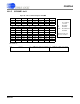
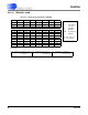
23.2.11 TBSCFG : 0x2A
(MSB) 23 22 21 20 19 18 17 16
INTP7 INTP6 INTP5 INTP4 INTP3 INTP2 INTP1 INTP0
R/WR/WR/WR/WR/WR/WR/WR/W
00000000
15 14 13 12 11 10 9 8
-- RATE2 RATE1 RATE0 TSYNC CDLY2 CDLY1 CDLY0
R/WR/WR/WR/WR/WR/WR/WR/W
00000000
7654321(LSB) 0
LOOP RUN DDLY5 DDLY4 DDLY3 DDLY2 DDLY1 DDLY0
R/WR/WR/WR/WR/WR/WR/WR/W
00000000
DF Address: 0x2A
-- Not defined;
read as 0
R Readable
W Writable
R/W Readable and
Writable
Bits in bottom rows
are reset condition
Figure 55. Test Bit Stream Configuration Register TBSCFG
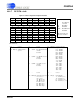
Bit definitions:
23:16 INTP[7:0] Interpolation factor
0xFF: 256
0xFE: 255
...
0x01: 2
0x00: 1 (use once)
15 -- Reserved 7 LOOP Loopback
TBSDATA output
to MDATA inputs
1: Enabled
0: Disabled
14:12 RATE[2:0] TBSDATA and
TBSCLK output
rate.
111: 2.048 MHz
110: 1.024 MHz
101: 512 kHz
100: 256 kHz
011: 128 kHz
010: 64 kHz
001: 32 kHz
000: 4 kHz
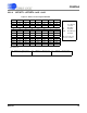
6 RUN Run Test Bit Stream
1: Enabled
0: Disabled
11 TSYNC Synchronization
1: Sync enabled
0: No sync
10:8 CDLY[2:0] TBSCLK output
phase delay
111: 7/8 period
110: 3/4 period
101: 5/8 period
100: 1/2 period
011: 3/8 period
010: 1/4 period
001: 1/8 period
000: none
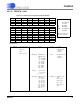
5:0 DDLY[5:0] TBSDATA output
delay
0x3F: 63 bits
0x3E: 62 bits
...
0x01: 1 bit
0x00: 0 bits ( no
delay)