
User guide


CS5376A
94 DS612F4
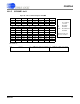
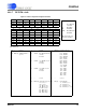
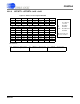
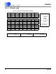
23.2.8 GAIN1 - GAIN4 : 0x21 - 0x24
(MSB) 23 22 21 20 19 18 17 16
GAIN23 GAIN22 GAIN21 GAIN20 GAIN19 GAIN18 GAIN17 GAIN16
R/WR/WR/WR/WR/WR/WR/WR/W
00000000
15 14 13 12 11 10 9 8
GAIN15 GAIN14 GAIN13 GAIN12 GAIN11 GAIN10 GAIN9 GAIN8
R/WR/WR/WR/WR/WR/WR/WR/W
00000000
7654321(LSB) 0
GAIN7 GAIN6 GAIN5 GAIN4 GAIN3 GAIN2 GAIN1 GAIN0
R/WR/WR/WR/WR/WR/WR/WR/W
00000000
DF Address: 0x21
-- Not defined;
read as 0
R Readable
W Writable
R/W Readable and
Writable
Bits in bottom rows
are reset condition
Figure 52. Gain Correction Register GAIN1
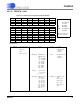
Bit definitions:
23:16 GAIN[23:16] Gain Correction
Upper Byte
15:8 GAIN[15:8] Gain Correction
Middle Byte
15:8 GAIN[7:0] Gain Correction
Lower Byte