
User guide

CS5376A
90 DS612F4
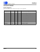
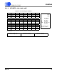
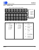
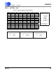
23.2.4 SPI2CTRL : 0x10
(MSB) 23 22 21 20 19 18 17 16
WOM SCKFS2 SCKFS1 SCKFS0 SPI2EN3 SPI2EN2 SPI2EN1 SPI2EN0
R/WR/WR/WR/WR/WR/WR/WR/W
00111111
15 14 13 12 11 10 9 8
RCH1 RCH0 D2SOP SCKPH SWEF SCKPO TM D2SREQ
R/WR/W R R/WR/WR/WR/WR/W
00000000
7654321(LSB) 0
DNUM2 DNUM1 DNUM0 CS4 CS3 CS2 CS1 CS0
R/WR/WR/WR/WR/WR/WR/WR/W
11100000
DF Address: 0x10
-- Not defined;
read as 0
R Readable
W Writable
R/W Readable
and Writable
Bits in bottom rows
are reset condition.
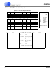
Bit definitions:
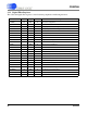
23 WOM Wired-or mode
1: Enabled (open drain)
0: Disabled (push-pull)
15:14 RCH
[1:0]
Read channel
11: SI4
10: SI3
01: SI2
00: SI1
7:5 DNUM
[2:0]
Number of bytes in
serial transaction
22:20 SCKFS
[2:0]
SCK2 frequency select
111: reserved
110: reserved
101: 4.096 MHz
100: 2.048 MHz
011: 1.024 MHz
010: 512 kHz
001: 128 kHz
000: 32 kHz
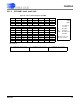
13 D2SOP Digital filter to SPI2
operation in progress
flag
4 CS4 Chip Select 4 Enable
12 SCKPH SO output timing
1: Data becomes valid
on first SCK2 edge
0: Data becomes valid
before first SCK2 edge
3 CS3 Chip Select 3 Enable
2 CS2 Chip Select 2 Enable
11 SWEF SPI2 write collision flag 1 CS1 Chip Select 1 Enable
19:16 SPI2EN
[3:0]
SI[4:1] input enable
1111: All enabled
0000: All disabled
10 SCKPO SCK2 data polarity
1: Valid on falling edge,
transition on rising edge
0: Valid on rising edge,
transition on falling edge
0 CS0 Chip Select 0 Enable
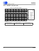
9 TM SPI2 timeout flag
1: SPI2 timed out
0: not timed out
8 D2SREQ Digital filter to SPI2
serial transaction request
1: Request operation
0: Operation complete
(cleared by hardware)
Figure 48. SPI 2 Control Register SPI2CTRL