
User guide

CS5376A
DS612F4 89
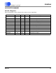
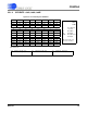
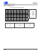
23.2.3 GPCFG1 : 0x0F
(MSB) 23 22 21 20 19 18 17 16
-- -- -- --
GP_DIR11 GP_DIR10 GP_DIR9 GP_DIR8
R/W R/W R/W R/W R/W R/W R/W R/W
00000000
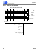
15 14 13 12 11 10 9 8
-- -- -- --
GP_PULL11 GP_PULL10 GP_PULL9 GP_PULL8
R/W R/W R/W R/W R/W R/W R/W R/W
00001111
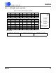
7654321(LSB) 0
-- -- -- --
GP_DATA11 GP_DATA10 GP_DATA9 GP_DATA8
R/W R/W R/W R/W R/W R/W R/W R/W
00001111
DF Address: 0x0F
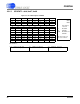
-- Not defined;
read as 0
R Readable
WWritable
R/W Readable and
Writable
Bits in bottom rows
are reset condition
Bit definitions:
Note: GPIO11 also used as boot EEPROM chip select EECS.
23:20 -- reserved 15:12 -- reserved 7:4 -- reserved
19:16 GP_DIR
[11:8]
GPIO pin direction
1: Output
0: Input
11:8 GP_PULL
[11:8]
GPIO pullup resistor
1: Enabled
0: Disabled
3:0 GP_DATA
[11:8]
GPIO data value
1: VDD
0: GND
Figure 47. GPIO Configuration Register GPCFG1