
User guide

CS5376A
DS612F4 18
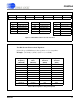
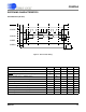
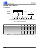
SWITCHING CHARACTERISTICS
Test Bit Stream (TBS)
5. TBSCLK phase can be delayed in 1/8 increments. The timing diagram shows no TBSCLK delay.
6. TBSDATA can be delayed from 0 to 63 full bit periods. The timing diagram shows no TBSDATA delay.
Parameter Symbol Min Typ Max Unit
TBS Clock Timing
TBS Clock Period t
1
-3.906- µs
TBS Clock High Time (Note 5) t
2
40 - 60 %
TBS Clock Low Time t
3
40 - 60 %
TBS Data Output Timing
TBS Data Bit Rate - 256 - kbps
TBS Data Rising to TBS Clock Rising Setup Time t
4
60 - - ns
TBS Clock Rising to TBS Data Falling Hold Time (Note 6) t
5
60 - - ns
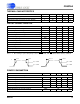
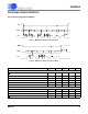
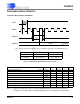
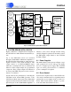
Figure 8. TBS Output Clock and Data Timing
TBSCLK
TBSDATA
MCLK
t
1
t
2
t
3
t
5
t
4
Note: Example timing shown for a 256 kHz output rate and no programmable delays.