CS5376A Low-power, Multi-channel Decimation Filter Features Description z 1- to 4-channel Digital Decimation Filter Multiple On-chip FIR and IIR Coefficient Sets Programmable Coefficients for Custom Filters Synchronous Operation The CS5376A is a multi-function digital filter utilizing a low-power signal processing architecture to achieve efficient filtering for up to four ∆Σ modulators.
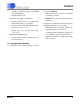
CS5376A TABLE OF CONTENTS 1. General Description . . . . . . . . . . . . . . . . . . . . . . . . . . . . . . . . . . . . . . 7 1.1. 1.2. 1.3. 1.4. Digital Filter Features . . . . . . . . . . . . . . . . . . . . . . . . . . . . . . . . . . . . . . . .7 Integrated Peripheral Features . . . . . . . . . . . . . . . . . . . . . . . . . . . . . . . .8 System Level Features . . . . . . . . . . . . . . . . . . . . . . . . . . . . . . . . . . . . . .8 Configuration Interface. . . . . . . . . . . . . . . . . . . . .
CS5376A 9.1. 9.2. 9.3. 9.4. 9.5. Pin Descriptions . . . . . . . . . . . . . . . . . . . . . . . . . . . . . . . . . . . . . . . . . . .32 Microcontroller Hardware Interface . . . . . . . . . . . . . . . . . . . . . . . . . . . .32 Microcontroller Serial Transactions . . . . . . . . . . . . . . . . . . . . . . . . . . . .32 Microcontroller Configuration Commands . . . . . . . . . . . . . . . . . . . . . . .35 Example Microcontroller Configuration . . . . . . . . . . . . . . . . . . . . . . . . .37 10.
CS5376A 17.7. TBS Synchronization . . . . . . . . . . . . . . . . . . . . . . . . . . . . . . . . . . . . . .66 18. Time Break Controller . . . . . . . . . . . . . . . . . . . . . . . . . . . . . . . . . . . 67 18.1. Pin Description . . . . . . . . . . . . . . . . . . . . . . . . . . . . . . . . . . . . . . . . . . .67 18.2. Time Break Operation . . . . . . . . . . . . . . . . . . . . . . . . . . . . . . . . . . . . .67 18.3. Time Break Delay. . . . . . . . . . . . . . . . . . . . . . . . . . . . . . . . .
CS5376A Figure 14. Figure 15. Figure 16. Figure 17. Figure 18. Figure 19. Figure 20. Figure 21. Figure 22. Figure 23. Figure 24. Figure 25. Figure 26. Figure 27. Figure 28. Figure 29. Figure 30. Figure 31. Figure 32. Figure 33. Figure 34. Figure 35. Figure 36. Figure 37. Figure 38. Figure 39. Figure 40. Figure 41. Figure 42. Figure 43. Figure 44. Figure 45. Figure 46. Figure 47. Figure 48. Figure 49. Figure 50. Figure 51. Figure 52. Figure 53. Figure 54. Figure 55. Figure 56. Figure 57. Figure 58.
CS5376A LIST OF TABLES Table 1. Microcontroller and EEPROM Configuration Commands . . . . . . . . . . .10 Table 2. TBS Configurations Using On-Chip Data . . . . . . . . . . . . . . . . . . . . . . .11 Table 3. SPI 1 and Digital Filter Registers . . . . . . . . . . . . . . . . . . . . . . . . . . . . .12 Table 4. Maximum EEPROM Configuration . . . . . . . . . . . . . . . . . . . . . . . . . . . .28 Table 5. EEPROM Boot Configuration Commands . . . . . . . . . . . . . . . . . . . . . .29 Table 6.
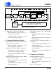
VDD2 (x2) VDD1 VD (x2) BOOT RESET SDTKI SDDAT SDRDY SDCLK CS5376A Clock and Synchronization Serial Data Output Port SPI 1 Serial Peripheral Interface 1 SSI SCK1 MISO MOSI SINT Time Break Controller TIMEB Test Bit Stream Controller Decimation and Filtering Engine GPIO General Purpose I/O TBSCLK TBSDATA GPIO11:EECS GPIO10 GPIO9 GPIO8 GPIO7 GPIO6 GPIO5 GPIO4:CS4 GPIO3:CS3 GPIO2:CS2 GPIO1:CS1 GPIO0:CS0 SCK2 SO SI1 SI2 SI3 SI4 GND2 (x2) GND1 GND (x2) MFLAG [4:1] MDATA [4:1] TDI SPI 2 Ser
CS5376A Modulator Input 512 kHz Sinc Filter 2 - 64000 FIR1 FIR2 4 Gain & DC Offset Corrections IIR1 st 2 1 Order IIR2 2 nd Order Output to High Speed Serial Data Port Output Word Rate from 4000 SPS ~ 1 SPS Figure 2. Digital Filtering Stages • Digital offset correction and calibration. - - Calibration engine for automatic calculation of offset correction factors. Dedicated TB status bit in the output data stream. - Programmable output delay to match system group delay.
CS5376A • alone boot EEPROM. - - Microcontroller boot permits reconfiguration during operation. - EEPROM boot sets a fixed operational configuration. 40 µW standby mode. Flexible power supply configurations. - • 37 mW for 4-channel operation at 500 SPS (9.25 mW/channel). Separate digital logic core, telemetry I/O, and modulator I/O power supplies. • Configuration commands written through Serial Peripheral Interface 1. (See Table 1) Telemetry I/O and modulator I/O interfaces operate from 3.
CS5376A Microcontroller Boot Configuration Commands Name CMD 24-bit DAT1 24-bit DAT2 24-bit Description NOP 000000 - - WRITE DF REGISTER 000001 REG DATA No Operation Write Digital Filter Register READ DF REGISTER 000002 REG [DATA] - Read Digital Filter Register WRITE FIR COEFFICIENTS 000003 NUM FIR1 (FIR COEF) NUM FIR2 (FIR COEF) Write Custom FIR Coefficients WRITE IIR COEFFICIENTS 000004 a11 b11 a22 b21 b10 a21 b20 b22 Write Custom IIR Coefficients WRITE ROM COEFFICIENTS 00000
CS5376A Bits 23:20 19:16 15:12 11:8 7:4 3:0 Selection 0000 0000 IIR2 IIR1 FIR2 FIR1 Bits 15:12 IIR2 Coefficients Bits 11:8 IIR1 Coefficients Bits 3:0 FIR1 Coefficients 0000 3 Hz @ 2000 SPS 0000 3 Hz @ 2000 SPS 0000 Linear Phase 0001 3 Hz @ 1000 SPS 0001 3 Hz @ 1000 SPS 0001 Minimum Phase 0010 3 Hz @ 500 SPS 0010 3 Hz @ 500 SPS 0011 3 Hz @ 333 SPS 0011 3 Hz @ 333 SPS Bits 7:4 FIR2 Coefficients 0100 3 Hz @ 250 SPS 0100 3 Hz @ 250 SPS 0000 Linear Phase 0001 Min
CS5376A SPI 1 Registers Addr. Type # Bits SPI1CTRL Name 00 - 02 R/W 8, 8, 8 SPI 1 Control Description SPI1CMD 03 - 05 R/W 8, 8, 8 SPI 1 Command SPI1DAT1 06 - 08 R/W 8, 8, 8 SPI 1 Data 1 SPI1DAT2 09 - 0B R/W 8, 8, 8 SPI 1 Data 2 Addr.
CS5376A 2. CHARACTERISTICS AND SPECIFICATIONS • Min / Max characteristics and specifications are guaranteed over the Specified Operating Conditions. • Typical performance characteristics and specifications are derived from measurements taken at nominal supply voltages and TA = 25°C. • GND, GND1, GND2 = 0 V, all voltages with respect to 0 V.
CS5376A THERMAL CHARACTERISTICS Parameter Symbol Min Typ Max Unit TJ - - 135 °C Junction to Ambient Thermal Impedance ΘJA - 65 Ambient Operating Temperature (Power Applied) TA -40 - +85 °C Symbol Min Typ Max Unit High-Level Input Drive Voltage VIH 0.6 * VDD - VDD V Low-Level Input Drive Voltage VIL 0.0 - 0.8 V Allowable Junction Temperature °C / W DIGITAL CHARACTERISTICS Parameter High-Level Output Drive Voltage Iout = -40 µA VOH VDD - 0.
CS5376A SWITCHING CHARACTERISTICS SPI 1 Interface Timing (External Master) SSI MOSI MSB LSB MSB - 1 t1 t2 t3 t4 t5 t6 SCK1 SCLK Figure 4. MOSI Write Timing in SPI Slave Mode SS I t 10 MISO MSB MSB - 1 t7 LSB t8 t9 SCK1 SCLK Figure 5.
CS5376A SWITCHING CHARACTERISTICS Serial Data Port (SD Port) SDRDY SDCLK t6 t3 t7 SDDAT t4 SDTKI SDTKO t5 t9 t8 t1 t2 t10 t11 Figure 6.
CS5376A SWITCHING CHARACTERISTICS CLK, SYNC, MCLK, MSYNC, and MDATAx SYNC MCLK MSYNC tmsd tmsh tmsd Data1 MDATAx Data2 Note: SYNC input latched on MCLK rising edge. MSYNC output triggered by MCLK falling edge. fMCLK 2.048 MHz 1.024 MHz tmsd = TMCLK / 4 tmsd = 122 ns tmsd = 244 ns tmsh = TMCLK tmsh = 488 ns tmsh = 976 ns Figure 7. SYNC, MCLK, MSYNC, MDATA Interface Timing Parameter Symbol Min Typ Max Unit CLK 32 32.
CS5376A SWITCHING CHARACTERISTICS Test Bit Stream (TBS) t1 t2 t3 TBSCLK TBSDATA t4 t5 MCLK Note: Example timing shown for a 256 kHz output rate and no programmable delays. Figure 8. TBS Output Clock and Data Timing Parameter Symbol Min Typ Max Unit t1 - 3.
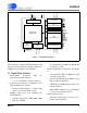
CS5376A Geophone or Hydrophone Sensor Geophone or Hydrophone Sensor M U X M U X CS3301A CS3302A CS5371A CS5372A AMP System Telemetry CS3301A CS3302A ∆Σ Modulator AMP CS5376A µController or Configuration EEPROM Digital Filter Geophone or Hydrophone Sensor Geophone or Hydrophone Sensor M U X M U X CS3301A CS3302A CS5371A CS5372A AMP CS3301A CS3302A Communication Interface ∆Σ Modulator AMP CS4373A Switch Switch MUX MUX Test DAC Figure 9. Multi-Channel System Block Diagram 3.
CS5376A 3.3 Clock Generation 3.7 Data Collection A single 32.768 MHz low-jitter clock input, which can be generated from a VCXO based PLL, is required to drive the CS5376A device. Clock inputs for other system devices are driven by clock outputs from the CS5376A. Data is collected from the CS5376A through the Serial Data port (SD port).
SDTKI SDTKO SDCLK SDRDY SDDAT SYNC CLK TIMEB BOOT RESET VDD1 GND1 SINT MOSI MISO SSI CS5376A 64 63 62 61 60 59 58 57 56 55 54 53 52 51 50 49 1 VDD1 Pad Ring 2 3 4 5 6 VD 7 Pad Ring 8 9 VD Pad Ring 10 11 12 13 14 15 VDD2 Pad Ring 16 17 18 19 20 21 22 23 24 25 26 27 28 29 30 31 32 CS5376A 48 47 46 45 44 43 42 41 40 39 38 37 36 35 34 33 SCK1 SSO GPIO11:EECS GPIO10 GPIO9 GPIO8 GPIO7 GPIO6 VD GND GND2 GPIO5 GPIO4:CS4 GPIO3:CS3 GPIO2:CS2 GPIO1:CS1 MDATA3 MFLAG3 MDATA2 MFLAG2 MDATA1 MFLAG1 GND GND2 VDD2 SI4
CS5376A VD, GND - Pins 7, 40, 6, 23, 39 Sets the operational voltage of the CS5376A logic core. Can be driven with voltages from 3 V to 5 V. A 3 V supply minimizes total power consumption. 4.2 Bypass Capacitors Each power supply pin should be bypassed with parallel 1 µF and 0.01 µF caps, or by a single 0.1 µF cap, placed as close as possible to the CS5376A. Bypass capacitors should be ceramic 22 (X7R, C0G), tantalum, or other good quality dielectric type. 4.
CS5376A RESET Self-Tests BOOT Pin 0 1 SELFTEST Register EEPROM Boot µController Boot Figure 11. Reset Control Block Diagram 5. RESET CONTROL The CS5376A reset signal is active low. When released, a series of self-tests are performed and the device either actively boots from an external EEPROM or enters an idle state waiting for microcontroller configuration. combined into the SELFTEST register (0x2F), with 0x0AAAAA indicating all passed.
CS5376A CLK Clock Divider and MCLK Generator Internal Clocks MCLK Output DSPCFG Register Figure 12. Clock Generation Block Diagram 6. CLOCK GENERATION The CS5376A requires a 32.768 MHz master clock input, which is used to generate internal digital filter clocks and external modulator clocks. ensure recovered clocks have identical phase, system PLL designs should use a phase/frequency detector architecture. 6.1 Pin Description 6.
CS5376A 0 SYNC 1 MSYNC Generator Digital Filter 1 MSYNC Output MSEN 0 Test Bit Stream TSYNC Figure 13. Synchronization Block Diagram 7. SYNCHRONIZATION The CS5376A has a dedicated SYNC input that aligns the internal digital filter phase and generates an external signal for synchronizing modulator analog sampling. By providing simultaneous rising edges to the SYNC pins of multiple CS5376A devices, synchronous sampling across a network can be guaranteed. phase.
CS5376A VD GPIO11:EECS SCK1 CS5376A MISO MOSI 46 1 48 6 50 2 51 5 CS 3 WP 8 7 VCC HOLD SCK AT25640 SO SI 4 GND Figure 14. EEPROM Configuration Block Diagram 8. CONFIGURATION BY EEPROM After reset, the CS5376A reads the state of the BOOT pin to determine a source for configuration commands. If BOOT is high, the CS5376A initiates serial transactions through the SPI 1 port to read configuration information from an external EEPROM. 8.
CS5376A Instruction Read Opcode Address 0x03 Definition ADDR[15:0] Read data beginning at the address given in ADDR. SPI 1 Read from EEPROM SSI READ CMD 0x03 MOSI 2 BYTE ADDR ADDR ADDR DATA1 DATA2 DATA3 MISO 1 BYTE / 3 BYTE DATA EECS Cycle 1 2 3 4 5 6 7 8 MSB 6 5 4 3 2 1 LSB 6 5 4 3 2 1 LSB SCK1 MOSI MISO MSB X EECS Figure 15.
CS5376A 0000h 0010h Mfg Header 8-bit Command N x 24-bit Data 8-bit Command N x 24-bit Data 1FFFh EEPROM Manufacturing Information EEPROM Command and Data Values Write DF Register - 0x01 This EEPROM command writes a data value to the specified digital filter register. Digital filter registers control hardware peripherals and filtering functions. See “Digital Filter Registers” on page 86 for the bit definitions of the digital filter registers.
CS5376A Sample Command: Sample Command: Write IIR1 coefficients 0x84BC9D, 0x7DA1B1, 0x825E4F, and IIR2 coefficients 0x83694F, 0x3CAD5F, 0x3E5104, 0x835DF8, 0x3E5104. Select IIR1 and IIR2 3 Hz @ 500 SPS low-cut coefficients, with FIR1 and FIR2 linear phase highcut coefficients. Data word 0x002200.
CS5376A Sample Command: Write test bit stream data 0x000000, 0x0007DA, 0x000FB5, 0x00178F. 05 00 00 04 00 00 00 00 07 DA 00 0F B5 00 17 8F Write TBS ROM Data - 0x06 This EEPROM command selects the on-chip test bit stream (TBS) data for use by the TBS generator. No data words are required for this EEPROM command. See “Test Bit Stream Generator” on page 64 for more information about the on-chip test bit stream data set.
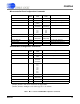
CS5376A Addr Data 00 00 01 02 Description Addr Data 20 00 00 21 02 00 22 40 03 00 23 01 04 00 24 00 05 00 25 00 06 00 26 2A 07 00 27 07 08 00 28 40 09 00 29 40 0A 00 2A 01 Mfg header 0B 00 2B 00 0C 00 2C 00 0D 00 2D 2B 0E 00 2E 04 0F 00 2F B0 10 04 30 00 31 07 11 00 12 22 Write ROM Coefficients 13 00 14 06 Write TBS ROM Data 15 01 Write CONFIG Register 16 00 17 00 18 00 19 07 1A 04 1B 31 1C 01 1D 00 1E
CS5376A Digital Filter Command Interpreter SPI 1 Registers SPI 1 Pin Logic SSI SCK1 MOSI MISO SINT Figure 17. Serial Peripheral Interface 1 (SPI 1) Block Diagram 9. CONFIGURATION BY MICROCONTROLLER After reset, the CS5376A reads the state of the BOOT pin to determine a source for configuration commands. If BOOT is low, the CS5376A receives configuration commands from a microcontroller. 9.1 Pin Descriptions Pins required for microcontroller boot are listed here, other SPI 1 pins are inactive. 9.
CS5376A Instruction Opcode Address Definition Write 0x02 ADDR[7:0] Write SPI 1 registers beginning at the address in ADDR. Read 0x03 ADDR[7:0] Read SPI 1 registers beginning at the address in ADDR. Microcontroller Write to SPI 1 SSI MOSI 0x02 ADDR Data1 Data2 DataN Data1 Data2 DataN MISO Microcontroller Read from SPI 1 SSI 0x03 MOSI ADDR MISO Cycle 1 2 3 4 5 6 7 8 MSB 6 5 4 3 2 1 LSB 6 5 4 3 2 1 LSB SCK1 MOSI MISO MSB X SSI Figure 18.
CS5376A 9.3.2 SPI 1 registers The SPI 1 registers are shown in Figure 19 and are 24-bit registers mapped into an 8-bit register space as high, mid, and low bytes. See “SPI 1 Registers” on page 81 for the bit definitions of the SPI 1 registers. 9.3.3 SPI 1 transactions A serial transaction to the SPI 1 registers starts with an SPI opcode, followed by an address, and then some number of data bytes written or read starting at that address.
CS5376A The E2DREQ bit reads high while a configuration command is being processed. When low, the digital filter is ready to receive a new configuration command. Sample Command: Write digital filter register 0x00 with data value 0x070431. Then write 0x20 with data 0x000240. 02 03 00 00 01 00 00 00 07 04 31 Delay 1 ms, monitor SINT, or poll E2DREQ 9.
CS5376A Delay 1 ms, monitor SINT, or poll E2DREQ Sample Command: MOSI: 03 06 00 00 00 Write IIR1 coefficients 0x84BC9D, 0x7DA1B1, 0x825E4F, and IIR2 coefficients 0x83694F, 0x3CAD5F, 0x3E5104, 0x835DF8, 0x3E5104. MISO: xx xx 07 04 31 02 03 00 00 02 00 00 20 Delay 1 ms, monitor SINT, or poll E2DREQ MOSI: 03 06 00 00 00 MISO: xx xx 00 02 40 Write FIR Coefficients - 0x03 This command writes custom coefficients for the FIR1 and FIR2 filters.
CS5376A on page 64 for information about using custom test bit stream data sets. Sample Command: Write test bit stream data 0x000000, 0x0007DA, 0x000FB5, 0x00178F. 02 03 00 00 06 00 00 04 Delay 1 ms, monitor SINT, or poll E2DREQ 02 06 00 00 00 00 07 DA Delay 1 ms, monitor SINT, or poll E2DREQ 02 06 00 0F B5 00 17 8F Delay 1 ms, monitor SINT, or poll E2DREQ Write TBS ROM Data - 0x07 This command selects the on-chip test bit stream (TBS) data for use by the TBS generator.
CS5376A Transaction SPI Data Description Write ROM coefficients 01 02 03 00 00 05 00 22 00 02 Delay 1ms, monitor SINT, or poll E2DREQ 03 02 03 00 00 07 04 Delay 1ms, monitor SINT, or poll E2DREQ 05 02 03 00 00 01 00 00 00 07 04 31 06 Delay 1ms, monitor SINT, or poll E2DREQ 07 02 03 00 00 01 00 00 20 00 02 40 08 Delay 1ms, monitor SINT, or poll E2DREQ 09 02 03 00 00 01 00 00 2A 07 40 40 10 Delay 1ms, monitor SINT, or poll E2DREQ 11 02 03 00 00 01 00 00 2B 04 B0 00 12 Delay 1ms, mon
CS5376A MCLK / MSYNC Generate MCLK MCLK/2 MSYNC MDATA[4:1] MDI Input MFLAG[4:1] 512 kHz CLK SYNC SINC Filter DC Offset & Gain Correction FIR Filters IIR Filter Output to High Speed Serial Data Port (SD Port) Output Rate 4000 SPS ~ 1 SPS Figure 20. Modulator Data Interface 10.MODULATOR INTERFACE The CS5376A performs digital filtering for up to four ∆Σ modulators. Signals from the modulators are connected through the modulator data interface (MDI). 10.2 Modulator Clock Generation 10.
CS5376A 10.4 Modulator Data Inputs 10.5 Modulator Flag Inputs The MDATA input expects 1-bit ∆Σ data at a 512 kHz or 256 kHz rate. The input rate is selected by a bit in the CONFIG register (0x00). By default, MDATA is expected at 512 kHz. A high MFLAG input signal indicates the corresponding ∆Σ modulator has become unstable due to an analog over-range input signal. Once the over-range signal is reduced, the modulator recovers stability and the MFLAG signal is cleared.
CS5376A Modulator Input 512 kHz SINC Filter 2 - 64000 FIR1 4 DC Offset & Gain Correction FIR2 IIR1 2 1st Order IIR2 2nd Order Output to High Speed Serial Data Port (SD Port) Output Rate 4000 SPS ~ 1 SPS Figure 21. Digital Filter Stages 11.DIGITAL FILTER INITIALIZATION The CS5376A digital filter consists of three multistage sections: a three stage SINC filter, a two stage FIR filter, and a two stage IIR filter.
CS5376A Bits 23:20 19:16 15:12 11:8 7:4 3:0 Selection 0000 0000 IIR2 IIR1 FIR2 FIR1 Bits 15:12 IIR2 Coefficients Bits 11:8 IIR1 Coefficients Bits 3:0 FIR1 Coefficients 0000 3 Hz @ 2000 SPS 0000 3 Hz @ 2000 SPS 0000 Linear Phase 0001 3 Hz @ 1000 SPS 0001 3 Hz @ 1000 SPS 0001 Minimum Phase 0010 3 Hz @ 500 SPS 0010 3 Hz @ 500 SPS 0011 3 Hz @ 333 SPS 0011 3 Hz @ 333 SPS Bits 7:4 FIR2 Coefficients 0100 3 Hz @ 250 SPS 0100 3 Hz @ 250 SPS 0000 Linear Phase 0001 Min
CS5376A 1-bit ∆−Σ Input 5th order sinc1 8 4th order sinc3 stage1 5 4th order sinc2 stage1 2 4th order sinc3 stage2 5 4th order sinc2 stage2 2 4th order sinc3 stage3 5 4th order sinc2 stage3 2 5th order sinc3 stage4 2 4th order sinc2 stage4 2 6th order sinc3 stage5 2 6th order sinc3 stage6 3 24-bit Output Figure 23. SINC Filter Block Diagram 12.SINC FILTER The SINC filters primary purpose is to attenuate out-of-band noise components from the ∆Σ modulators.
CS5376A SINC1 – Single stage, fixed decimate by 8 5th order decimate by 8, 36 coefficients SINC2 – Multi-stage, variable decimation Stage Stage Stage Stage 1: 2: 3: 4: 4th 4th 5th 6th order order order order decimate decimate decimate decimate by by by by 2, 2, 2, 2, 5 5 6 7 coefficients coefficients coefficients coefficients SINC3 – Multi-stage, variable decimation Stage Stage Stage Stage Stage Stage 1: 2: 3: 4: 5: 6: 4th 4th 4th 5th 6th 6th order order order order order order decimate decima
CS5376A Filter Type System Function SINC1 5th order decimate by 8 36 coefficients ⎛ 1 − z −8 ⎞ ⎟ H ( z ) = ⎜⎜ −1 ⎟ ⎝1− z ⎠ Filter Type System Function SINC2 (Stage 1) SINC2 (Stage 2) 4th order decimate by 2 5 coefficients ⎛ 1 − z −2 ⎞ ⎟ H ( z ) = ⎜⎜ −1 ⎟ ⎝1− z ⎠ 4 h0 h1 h2 h3 h4 = = = = = 1 4 6 4 1 SINC2 (Stage 3) 5th order decimate by 2 6 coefficients ⎛ 1 − z −2 ⎞ ⎟ H ( z ) = ⎜⎜ −1 ⎟ ⎝1− z ⎠ 5 h0 h1 h2 h3 h4 h5 = = = = = = 1 5 10 10 5 1 SINC2 (Stage 4) 6th order decimate by 2 7 coefficie
CS5376A Filter Type System Function Filter Coefficients SINC3 (Stage 1) SINC3 (Stage 2) SINC3 (Stage 3) 4th order decimate by 5 17 coefficients ⎛ 1 − z −5 ⎞ ⎟ H ( z ) = ⎜⎜ −1 ⎟ ⎝1− z ⎠ 4 h0 h1 h2 h3 h4 h5 h6 h7 h8 h9 h10 h11 h12 h13 h14 h15 h16 = = = = = = = = = = = = = = = = = 1 4 10 20 35 52 68 80 85 80 68 52 35 20 10 4 1 SINC3 (Stage 4) 5th order decimate by 2 6 coefficients ⎛ 1 − z −2 ⎞ ⎟ H ( z ) = ⎜⎜ −1 ⎟ 1 z − ⎠ ⎝ 5 h0 h1 h2 h3 h4 h5 = = = = = = 1 5 10 10 5 1 SINC3 (Stage 5) 6th order
CS5376A FIR1 Filter - decimate by 4 FIR2 Filter - decimate by 2 Figure 25. FIR Filter Block Diagram 13.FIR FILTER The finite impulse response (FIR) filter block consists of two cascaded stages, FIR1 and FIR2. It compensates for SINC filter droop and creates a low-pass corner to block aliased components of the input signal. On-chip linear phase or minimum phase coefficients can be selected using a configuration command, or the coefficients can be programmed for a custom filter response. 13.
CS5376A 13.4 Programmable FIR Coefficients A maximum of 255 + 255 coefficients can be programmed into FIR1 and FIR2 to create a custom filter response. The total number of coefficients for the FIR filter is fundamentally limited by the available computation cycles in the digital filter, which itself is determined by the digital filter clock rate. Custom filter sets should normalize the maximum coefficient value to 24-bit two’s complement full scale, 0x7FFFFF, and scale all other coefficients accordingly.
CS5376A FIR1 – Single stage, fixed decimate by 4 Coefficient set 0: linear phase decimate by 4, 48 coefficients Coefficient set 1: minimum phase decimate by 4, 48 coefficients SINC droop compensation filter FIR2 – Single stage, fixed decimate by 2 Coefficient set 0: linear phase decimate by 2, 126 coefficients Coefficient set 1: minimum phase decimate by 2, 126 coefficients Brick wall low-pass filter, flat to 40% fs Combined SINC + FIR digital filter specifications Passband ripple less than +/- 0.
CS5376A Individual filter stage group delay (no IIR) Decimation Ratios 8 36 Group Delay (Filter Stage Input Rate) 17.5 2 2,2 2,2,2 2,2,2,2 7 6,7 5,6,7 5,5,6,7 3.0 8.5 19.0 40.0 3 2 2,2 5,2,2 5,5,2,2 5,5,5,2,2 13 7 6,7 17,6,7 17,17,6,7 17,17,17,6,7 6.0 3.0 8.5 50.5 260.5 1310.5 Coefficient Set 0 Coefficient Set 1 4 4 48 48 23.5 See Figure Coefficient Set 0 Coefficient Set 1 2 2 126 126 62.
CS5376A Minimum phase group delay FIR1 Minimum Phase Group Delay (Normalized frequency) FIR2 Minimum Phase Group Delay (Normalized frequency) Figure 27.
CS5376A Filter Type FIR1 (Coefficient set 0) Low pass, SINC compensation Linear phase decimate by 4 48 coefficients FIR1 (Coefficient set 1) Low pass, SINC compensation Minimum phase decimate by 4 48 coefficients Filter Coefficients (normalized 24-bit) h24 h0 = 558 h25 h1 = 1905 h26 h2 = 3834 h27 h3 = 5118 h28 h4 = 365 h29 h5 = -14518 h30 h6 = -39787 h31 h7 = -67365 h32 h8 = -69909 h33 h9 = -19450 h34 h10 = 97434 h35 h11 = 258881 h36 h12 = 375562 h37 h13 = 332367 h38 h14 = 39864 h39 h15 = -496361 h40 h16
CS5376A Filter Type Filter Coefficients (normalized 24-bit) FIR2 (Coefficient set 0) Low pass, passband to 40% fs Linear phase decimate by 2 126 coefficients h0 h1 h2 h3 h4 h5 h6 h7 h8 h9 h10 h11 h12 h13 h14 h15 h16 h17 h18 h19 h20 h21 h22 h23 h24 h25 h26 h27 h28 h29 h30 h31 h32 h33 h34 h35 h36 h37 h38 h39 h40 h41 h42 h43 h44 h45 h46 h47 h48 h49 h50 h51 h52 h53 h54 h55 h56 h57 h58 h59 h60 h61 h62 = = = = = = = = = = = = = = = = = = = = = = = = = = = = = = = = = = = = = = = = = = = = = = = = = = = = = =
CS5376A Filter Type Filter Coefficients (normalized 24-bit) FIR2 (Coefficient set 1) Low pass, passband to 40% fs Minimum phase decimate by 2 126 coefficients h0 h1 h2 h3 h4 h5 h6 h7 h8 h9 h10 h11 h12 h13 h14 h15 h16 h17 h18 h19 h20 h21 h22 h23 h24 h25 h26 h27 h28 h29 h30 h31 h32 h33 h34 h35 h36 h37 h38 h39 h40 h41 h42 h43 h44 h45 h46 h47 h48 h49 h50 h51 h52 h53 h54 h55 h56 h57 h58 h59 h60 h61 h62 = = = = = = = = = = = = = = = = = = = = = = = = = = = = = = = = = = = = = = = = = = = = = = = = = = = = = =
CS5376A 1st Order IIR1 2nd Order IIR2 b10 b20 Z-1 Z-1 -a11 b11 -a21 b21 Z-1 3rd Order IIR3 implemented by running both IIR1 and IIR2 stages -a22 b22 Figure 28. IIR Filter Block Diagram 14.IIR FILTER The infinite impulse response (IIR) filter block consists of two cascaded stages, IIR1 and IIR2. It creates a high-pass corner to block very low-frequency and DC components of the input signal.
CS5376A characteristic equations model the operation of the 2nd order IIR filter with unnormalized coefficients. W5 = W4 W4 = W3 Which on-chip coefficient set to use is selected by a data word following the ‘Write ROM Coefficients’ configuration command. See “Filter Coefficient Selection” on page 41 for information about selecting on-chip coefficient sets. W3 = X + (-a21 * W4) + (-a22 * W5) Y = (W3 * b20) + (W4 * b21) + (W5 * b22) 14.
CS5376A IIR1 – Single stage, no decimation 1st order no decimation, 3 coefficients Coefficient Coefficient Coefficient Coefficient Coefficient set set set set set 0: 1: 2: 3: 4: high-pass, high-pass, high-pass, high-pass, high-pass, corner corner corner corner corner 0.15% 0.30% 0.60% 0.90% 1.
CS5376A Filter Type System Function Filter Coefficients (normalized 24-bit) a11 = -8309916 b10 = 8349262 b11 = -8349262 IIR1 (Coefficient set 0) 1st order, high pass Corner at 0.15% fs 3 coefficients ⎛ b + b z −1 ⎞ H ( z ) = ⎜⎜ 10 11 −1 ⎟⎟ ⎝ 1 + a11 z ⎠ IIR1 (Coefficient set 1) 1st order, high pass Corner at 0.30% fs 3 coefficients ⎛ b + b z −1 ⎞ H ( z ) = ⎜⎜ 10 11 −1 ⎟⎟ ⎝ 1 + a11 z ⎠ a11 = -8231957 b10 = 8310282 b11 = -8310282 IIR1 (Coefficient set 2) 1st order, high pass Corner at 0.
CS5376A MDI Input 512 kHz SINC Filter FIR Filters 4 Output to High Speed Serial Data Port (SD Port) Output Rate 4000 SPS ~ 1 SPS IIR Filter 4 Gain Correction 4 Offset Correction Offset Calibration 4 Figure 30. Gain and Offset Correction 15.GAIN AND OFFSET CORRECTION The CS5376A digital filter can apply independent gain and offset corrections to the data of each measurement channel. Also, an offset calibration algorithm can automatically calculate offset correction values for each channel.
CS5376A value in the OFFSETx registers (0x25-0x28) from the digital filter output data word. Offset correction values are 24-bit two’s complement with a maximum positive value of 0x7FFFFF, and a maximum negative value of 0x800000. If applying an offset correction causes the final result to exceed a 24-bit two’s complement maximum, the output data will saturate to that maximum value.
CS5376A System Telemetry Token Out Data Ready Clock Out Data In Token In CS5376A SDTKI SDRDY SDCLK SDDAT SDTKO Figure 31. Serial Data Port Block Diagram 16.SERIAL DATA PORT Once digital filtering is complete, each 24-bit output sample is combined with an 8-bit status byte. These 32-bit data words are written to an 8-deep FIFO buffer and then transmitted to the communications channel through a high speed serial data port (SD port). 16.2 SD Port Data Format 16.
CS5376A Status Word 2 Word 1 Data Word 3 Word 4 128 bits 31 23 0 Status MFLAG 31 -30 0 - Modulator Ok 1 - Modulator Error CH[1] 29 Data CH[0] 28 00 - Channel 1 01 - Channel 2 10 - Channel 3 11 - Channel 4 TB -27 26 W 24 -25 0 - No Time Break 1 - Time Break 0 - FIFO Ok 1 - FIFO Overflow Figure 32. SD Port Data Format BRK digital filter register (0x29) programs the sample delay for the TB bit output. See “Time Break Controller” on page 67 for more information about time break.
CS5376A SDTKI SDTKO SDRDY SDCLK SDDAT LSB MSB Figure 33. SD Port Transaction data is read from the SD port data FIFO, SDRDY is released and SDTKO is pulsed high for 100 nS. 16.3.2 Continuous Mode To have the CS5376A automatically initiate SD port transactions whenever data becomes available, connect SDTKI to a 4 MHz or slower clock source such as MCLK/2.
CS5376A Digital Filter Data Bus 24-bit TBSGAIN Register TBSCFG Register 24-bit Digital ∆Σ Modulator Clock Generation 1-bit TBSDATA TBSCLK Figure 34. Test Bit Stream Generator Block Diagram 17.TEST BIT STREAM GENERATOR The CS5376A test bit stream (TBS) generator creates sine wave ∆Σ bit stream data to drive an external test DAC. The TBS digital output can also be internally connected to the MDATA inputs for loopback testing of the digital filter. 17.
CS5376A Test Bit Stream Characteristic Equation: (Signal Freq) * (# TBS Data) * (Interpolation + 1) = Output Rate Example: (31.25 Hz) * (1024) * (0x07 + 1) = 256 kHz Signal Frequency (TBSDATA) Output Rate (TBSCLK) Output Rate Selection (RATE) Interpolation Selection (INTP) 10.00 Hz 256 kHz 0x4 0x18 10.00 Hz 512 kHz 0x5 0x31 25.00 Hz 256 kHz 0x4 0x09 25.00 Hz 512 kHz 0x5 0x13 31.25 Hz 256 kHz 0x4 0x07 31.25 Hz 512 kHz 0x5 0x0F 50.00 Hz 256 kHz 0x4 0x04 50.
CS5376A set can be written into the CS5376A. The number of data points to write, up to a maximum of 1024, depends on the required test signal frequency, output rate, and available interpolation factors. Custom data sets must be continuous on the ends; i.e. when copied end-to-end the data set must produce a smooth curve. 17.5 TBS Sine Wave Output The TBS generator uses data from digital filter memory to create a sine wave test signal that can drive a test DAC.
CS5376A TIMEBRK Delay Counter TIMEB TB Flag in SD Port Status Byte Figure 35. Time Break Block Diagram 18.TIME BREAK CONTROLLER A time break signal is used to mark timing events that occur during measurement. An external signal sets a flag in the status byte of an output sample to mark when the external event occurred. 18.3 Time Break Delay A rising edge input to the TIMEB pin causes the TB timing reference flag to be set in the SD port status byte.
CS5376A GP_PULL Pull Up Logic R CS output from SPI Data bit GPIO/CS GP_DATA GP_DIR Figure 36. GPIO Bi-directional Structure 19.GENERAL PURPOSE I/O The General Purpose I/O (GPIO) block provides 12 general purpose pins to interface with external hardware. sponding GPIO pin should be initialized as output mode and logical 1 to produce the chip select falling edge. 19.1 Pin Descriptions 19.3 GPIO Registers GPIO[4:0]:CS[4:0] - Pins 32 - 36 Standard GPIO pins also used as SPI 2 chip selects.
CS5376A Any GPIO pin can be used as an open-drain output by setting the data value to 0, enabling the pull-up, and using the GP_DIR direction bits to control the pin value. This open-drain output configuration uses the internal pull-up resistor to hold the pin high when GP_DIR is set as an input, and drives the pin low when GP_DIR is set as an output. 19.5.
CS5376A Pin logic Digital 4:1 Filter SPI2EN[4:1] / RCH[1:0] CS[4:0] Select logic CS0 CS1 CS2 CS3 CS4 To GPIO Block SCK2 SO SI1 SI2 SI3 SI4 SCKFS[2:0] / SCKPO / SCKPH Figure 37. Serial Peripheral Interface 2 (SPI 2) Block Diagram 20.SERIAL PERIPHERAL INTERFACE 2 The Serial Peripheral Interface 2 (SPI 2) port is a master mode SPI port designed to interface with serial peripherals. By writing the SPI2 digital filter registers, multiple serial slave devices can be controlled through the CS5376A.
CS5376A 20.3.1 SPI 2 Control Register The SPI 2 hardware is configured by the SPI2CTRL digital filter register (0x10). ports all four SPI modes, with mode 0 and mode 3 the most commonly used. Supported modes are: Bits in this register select the serial input pin and chip select pin used for a transaction, set the total number of bytes in a transaction, initiate a serial transaction, and report status information about a transaction.
CS5376A During a transaction, bits in SPI2CMD are output MSB first, with data in SPI2DAT written or read following. 20.3.3 SPI 2 Data Register The SPI2DAT register (0x12) is a 24-bit digital filter register containing three SPI data bytes. Data in SPI2DAT is always LSB aligned, with 1-byte data written or received using the low byte, 2-byte data written or received using the middle and low bytes, and 3-byte data written or received using all three bytes.
CS5376A Instruction Opcode Address Definition Write 0x02 SPI2CMD[7:0] Write serial peripheral beginning at the address given in SPI2CMD[7:0]. Read 0x03 SPI2CMD[7:0] Read serial peripheral beginning at the address given in SPI2CMD[7:0]. SPI 2 Write to External Slave SPI2CMD[15:8] SPI2CMD[7:0] SPI2DAT SO 0x02 ADDR Data1 Data2 Data3 Data1 Data2 Data3 SI CS SPI 2 Read from External Slave SPI2CMD[15:8] SPI2CMD[7:0] SO 0x03 ADDR SI SPI2DAT CS Figure 38.
CS5376A SPI 2 Transaction with SCKPH=0 Cycle SCK2 SCKPO = 0 SCK2 SCKPO = 1 SO SI 1 2 3 4 5 6 7 8 MSB 6 5 4 3 2 1 LSB 6 5 4 3 2 1 LSB MSB X Slave devices only drive SI after being selected and responding to a read command. CS SPI 2 Transaction with SCKPH=1 Cycle SCK2 SCKPO = 0 SCK2 SCKPO = 1 SO SI X 1 2 3 4 5 6 7 8 MSB 6 5 4 3 2 1 LSB MSB 6 5 4 3 2 1 LSB Slave devices only drive SI after being selected and responding to a read command.
CS5376A TRST TAP Controller TMS TDO TCK TDI Boundary Scan Cells Figure 40. JTAG Block Diagram 21.BOUNDARY SCAN JTAG The CS5376A includes an IEEE 1149.1 boundary scan JTAG port to test PCB interconnections. Refer to the IEEE 1149.1 specification for more information about boundary scan testing. 21.1 Pin Descriptions TRST - Pin 1 Reset input for the test access port (TAP) controller and all boundary scan cells, active low. Connect to GND to disable the JTAG port.
CS5376A 21.2.1 JTAG Reset As required by the IEEE 1149.1 specification, the JTAG TRST signal is independent of the CS5376A RESET signal. In systems not using the JTAG port, TRST should be connected to ground. In systems using the JTAG port, TRST and RESET should be independently driven to provide reset capability during boundry scan. 21.2.2 TAP Controller The test access port (TAP) controller manages commands and data through the boundary scan chain.
CS5376A BRC Pin Function BRC 1 TBSCLK data out 36 2 TBSDATA data out 3 DNC data out 4 MCLK/2 data out 39 5 MCLK data out 40 6 MSYNC data out 7 MDATA4 data in 8 MFLAG4 data in 43 9 MDATA3 data in 44 10 MFLAG3 data in 11 MDATA2 data in 12 MFLAG2 data in 47 13 MDATA1 data in 48 14 MFLAG1 data in 15 GND data in 16 SI4 data in 51 17 SI3 data in 52 18 SI2 data in 19 SI1 data in 20 SO 21 22 SCK2 23 24 BRC Pin GPIO11 Function 68 37 dat
CS5376A 22.DEVICE REVISION HISTORY The CS5376A is a pin compatible upgrade to the CS5376. The part family has had three revisions: CS5376 rev A CS5376 rev B CS5376A rev A The part number change for CS5376A reflects additional functionality built into the device. 22.1 Changes from CS5376 rev A to CS5376 rev B New Sinc Filter, SINC3 Added a new sinc filter, SINC3, between the previous sinc filters and FIR1. Will permit higher decimation rates for seismology applications. Not used for 0.25 ms, 0.
CS5376A Modified SINC2 filter to correct gain and timing errors Corrected SINC2 decimate by 2 gain error which affected 4000 SPS operation. Also modified SINC2 decimate by 16 output timing to match output of other SINC2 rates. Previous SINC2 decimate by 16 output was one sample later than expected. Corrected gain error of 333 SPS output rate SINC architecture was modified to correct gain error in SINC2 decimate by 12 by moving decimate by 3 stage into SINC3.
CS5376A Added Test Bit Stream (TBS) synchronization in sine wave mode. The TBS sine wave phase will reset if bit 11 of the TBSCFG register is set (TBSCFG bit 11 = 1) and a rising edge is received on the SYNC pin. When TBSCFG bit 11 is set low (TBSCFG bit 11 = 0), TBS phase is unaffected by the SYNC input similar to CS5376 revision A/B. Modified Time Break delay function.
CS5376A 23.REGISTER SUMMARY 23.1 SPI 1 Registers The CS5376A SPI 1 registers interface the serial port to the digital filter. Name Addr.
CS5376A 23.1.1 SPI1CTRL : 0x00, 0x01, 0x02 Figure 41.
CS5376A 23.1.2 SPI1CMD : 0x03, 0x04, 0x05 Figure 42.
CS5376A 23.1.3 SPI1DAT1 : 0x06, 0x07, 0x08 Figure 43.
CS5376A 23.1.4 SPI1DAT2 : 0x09, 0x0A, 0x0B Figure 44.
CS5376A 23.2 Digital Filter Registers The CS5376A digital filter registers control hardware peripherals and filtering functions. Name Addr.
CS5376A 23.2.1 CONFIG : 0x00 Figure 45.
CS5376A 23.2.2 GPCFG0 : 0x0E Figure 46.
CS5376A 23.2.3 GPCFG1 : 0x0F Figure 47.
CS5376A 23.2.4 SPI2CTRL : 0x10 Figure 48.
CS5376A 23.2.5 SPI2CMD : 0x11 Figure 49.
CS5376A 23.2.6 SPI2DAT : 0x12 Figure 50.
CS5376A 23.2.7 FILTCFG : 0x20 Figure 51.
CS5376A 23.2.8 GAIN1 - GAIN4 : 0x21 - 0x24 Figure 52.
CS5376A 23.2.9 OFFSET1 - OFFSET4 : 0x25 - 0x28 Figure 53.
CS5376A 23.2.10 TIMEBRK : 0x29 Figure 54.
CS5376A 23.2.11 TBSCFG : 0x2A Figure 55.
CS5376A 23.2.12 TBSGAIN : 0x2B Figure 56.
CS5376A 23.2.13 SYSTEM1, SYSTEM2 : 0x2C, 0x2D Figure 57.
CS5376A 23.2.14 VERSION : 0x2E Figure 58.
CS5376A 23.2.15 SELFTEST : 0x2F Figure 59.
CS5376A 24.
CS5376A Pin Name Pin Number Pin Type Pin Description 1 Input JTAG reset, active low. Connect to GND if JTAG is not used. JTAG port TRST TMS 2 Input JTAG test mode select. TCK 3 Input JTAG clock input. TDI 4 Input JTAG data input. TDO 5 Output JTAG data output. TBSCLK 8 Output Test bit stream clock output. TBSDATA 9 Output Test bit stream data output. DNC 10 N/A MCLK/2 12 Output Modulator clock output, half rate. Test Bit Stream No Connect Do not connect.
CS5376A Pin Name Pin Number Pin Type CLK 58 Input SYNC 59 Input Pin Description Clock and Synchronization Clock input, nominal 32.768 MHz. Sync input. Serial Data Port SDDAT SDRDY 60 Output SD port data output. 61 Output SD port data ready, active low. Open drain output requiring a 10 kΩ pull-up. SDCLK 62 Input SD port clock input. SDTKO 63 Output SD port token output. SDTKI 64 Input SD port token input.
CS5376A 25.PACKAGE DIMENSIONS 64L TQFP PACKAGE DRAWING E E1 D D1 1 e B ∝ A A1 L DIM A A1 B D D1 E E1 e* L µ DS612F4 INCHES MILLIMETERS MIN MAX MIN MAX --0.063 --1.60 0.002 0.006 0.05 0.15 0.007 0.011 0.17 0.27 0.461 0.484 11.70 12.30 0.390 0.398 9.90 10.10 0.461 0.484 11.70 12.30 0.390 0.398 9.90 10.10 0.016 0.024 0.40 0.60 0.018 0.030 0.45 0.75 0.000° 7.000° 0.00° 7.00° * Nominal pin pitch is 0.50 mm Controlling dimension is mm.
CS5376A 26.ORDERING INFORMATION Model Temperature Package -40 to +85 °C 64-pin TQFP CS5376A-IQ CS5376A-IQZ Lead Free 27.ENVIRONMENTAL, MANUFACTURING, & HANDLING INFORMATION Model Number Peak Reflow Temp CS5376A-IQ 240 °C CS5376A-IQZ Lead Free 250 °C MSL Rating* Max Floor Life 3 7 Days * MSL (Moisture Sensitivity Level) as specified by IPC/JEDEC J-STD-020. 28.REVISION HISTORY Revision Date Changes PP1 SEP 2003 Initial “Preliminary Product” release.