
Instruction Manual

CS5374
CS5374
5
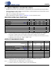
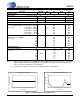
THERMAL CHARACTERISTICS
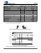
ANALOG CHARACTERISTICS
Notes: 7. Common mode signals pass through the differential amplifier architecture and are rejected by the
modulator CMRR.
8. Output impedance characteristics are approximate and can vary up to ±30% depending on process
parameters.
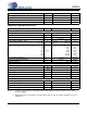
Parameter Symbol Min Typ Max Unit
Ambient Operating Temperature T
A
-10 - 70 °C
Storage Temperature Range T
STR
-65 - 150 °C
Allowable Junction Temperature T
JCT
--125°C
Junction to Ambient Thermal Impedance (4-layer PCB) θ
JA
-26-°C/W
Parameter Symbol Min Typ Max Unit
Amplifier Inputs
Signal Frequencies BW DC - 2000 Hz
Differential Gain GAIN x1 - x64
Common Mode Gain (Note 7) GAIN
CM
-x1-
Common Mode Voltage V
cm
-
(VA-)+2.5
-V
Voltage Range (Signal + Vcm) x1
x2 - x64
V
IN
(VA-)+0.7
(VA-)+0.7
-
-
(VA+)-1.25
(VA+)-1.75
V
Full Scale Differential Input x1
x2
x4
x8
x16
x32
x64
V
INFS
-
-
-
-
-
-
-
-
-
-
-
-
-
-
5
2.5
1.25
625
312.5
156.25
78.125
V
pp
V
pp
V
pp
mV
pp
mV
pp
mV
pp
mV
pp
Differential Input Impedance Z
INDIFF
-1, 20- TΩ, pF
Common Mode Input Impedance Z
INCM
- 0.5, 40 - TΩ, pF
Input Bias Current I
IN
-140pA
Amplifier Outputs
Full Scale Output, Differential V
OUT
--5V
pp
Output Voltage Range (Signal + Vcm) V
RNG
(VA-)+0.5
-
(VA+)-0.5
V
Output Impedance (Note 8)Z
OUT
-40- Ω
Output Impedance Drift (Note 8)Z
TC
-0.38- Ω/°C
Output Current I
OUT
--+25 mA
Load Capacitance C
L
--100nF
Guard Outputs
Guard Output Voltage V
GUARD
-V
cm
-V
Guard Output Impedance (Note 8)ZG
OUT
-500- Ω
Guard Output Current IG
OUT
--40μA
Guard Load Capacitance CG
L
--100pF