
Instruction Manual

CS5374
CS5374
38
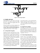
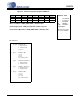
9.4 ADCCFG: 0x03
9.5 PWRCFG: 0x04
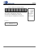
(MSB)7654321(LSB)0
OFST
HP PWDN2 PWDN1 --- --- --- ---
R/W R/W R/W R/W R/W R/W R/W R/W
00000000
Figure 23. Modulator 1 & 2 Configuration Register ADCCFG
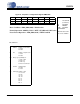
Bit definitions:
7OFSTModulator Offset
(add -60mV to Channel 1,
add -35mV to Channel 2)
1: disable
0: enable
6 HP Modulator High Precision
1: enable
0: disable
5 PWDN2 Modulator 2 Power Down
1: enable
0: disable
4 PWDN1 Modulator 1 Power Down
1: enable
0: disable
3:0 --- Reserved
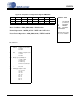
Address: 0x03
-- Not defined
(read as 0)
R Readable
WWritable
R/W Readable
and Writable
Bits in bottom rows
are reset condition
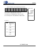
Reset Condition : 0000_0000 (0x00) : Default value
Normal Operation : 0100_0000 (0x40) : HP mode enabled
Power Down Operation : 0011_0000 (0x30) : PWDN enabled