
User Manual

CS5371A CS5372A
DS748F3 9
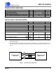
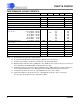
DIGITAL CHARACTERISTICS
Notes: 19. Device is intended to be driven with CMOS logic levels.
Parameter Symbol Min Typ Max Unit
Digital Inputs
High-level Input Voltage (Note 9, 19)V
IH
0.6*VD - VD V
Low-level Input Voltage (Note 9, 19)V
IL
0.0 - 0.8 V
Input Leakage Current I
IN
-±1±10μA
Digital Input Capacitance (Note 9) C
IN
-9- pF
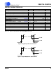
Input Rise Times Except MCLK (Note 9) t
RISE
--100ns
Input Fall Times Except MCLK (Note 9) t
FALL
--100ns
Digital Outputs
High-level Output Voltage, I
out
=-40μA(Note 9)V
OH
VD - 0.3 - - V
Low-level Output Voltage, I
out
=40μA(Note 9)V
OL
--0.3V
High-Z Leakage Current I
OZ
--±10μA
Digital Output Capacitance (Note 9) C
OUT
-9- pF
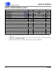
Output Rise Times (Note 9) t
RISE
--100ns
Output Fall Times (Note 9) t
FALL
--100ns
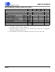
0.9 * VD
0.1 * VD
t
fall
t
rise
Figure 4. Digital Input Rise and Fall Times
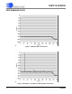
0.9 * VD
0.1 * VD
t
fall
t
rise
Figure 5. Digital Output Rise and Fall Times