
User Manual

CS5371A CS5372A
16 DS748F3
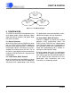
4. ANALOG SIGNALS
The CS5371A and CS5372A modulators have
differential analog inputs which are separated
into rough and fine charge differential pairs
(INR±, INF±) to maximize sampling accuracy.
Both sets of modulator inputs require a simple
differential anti-alias RC filter to ensure high-
frequency signals do not alias into the mea-
surement bandwidth.
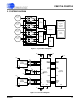
4.1 INR±, INF± Modulator Inputs
The modulator analog inputs are separated
into differential rough and fine signals (INR±,
INF±). The positive half of the differential input
signal is connected to INR+ and INF+, while
the negative half is attached to INF- and INR-.
The INR± pins are switched-capacitor ‘rough
charge’ inputs that pre-charge the internal an-
alog sampling capacitor before it is connected
to the INF± fine input pins.
4.2 Input Impedance
The modulator inputs have a dynamic
switched-capacitor architecture and so have a
rough charge input impedance that is inversely
proportional to the input master clock frequen-
cy and the input capacitor size, [1 / (f x C)].
Internal to the modulator, the rough inputs
(INR±) pre-charge the sampling capacitor
used by the fine inputs (INF±), therefore the in-
put current to the fine inputs is typically very
low and the effective input impedance is or-
ders of magnitude above the impedance of the
rough inputs.
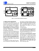
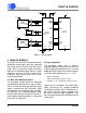
CS5372A
ΔΣ Modulator
INF+
INR+
INF-
INR-
INF-
INR-
INF+
INR+
VREF+
VREF-
VA+
VA-
VD
GND
MDATA1
MFLAG1
MDATA2
MFLAG2
MCLK
MSYNC
PWDN1
OFST
PWDN2
VREF
2.5 V
VA+
VA-
10 Ω
0.01μF
VD
CS5376A
Digital Filter
VDD2
GND
MDATA1
MFLAG1
MDATA2
MFLAG2
MCLK
MSYNC
GPIO
GPIO
GPIO
VA+
0.1μF 0.01μF
VD
VA-
0.1μF
20nF
C0G
20nF
C0G
680
CS3301A
CS3302A
AMPLIFIER
OUTR+
OUTF+
OUTF-
OUTR-
680
680
680
20nF
C0G
20nF
C0G
680
CS3301A
CS3302A
AMPLIFIER
OUTR+
OUTF+
OUTF-
OUTR-
680
680
680
VA+
VA+
VA-
VA-
VA+
VA+
VA-
VA-
100μF
Figure 11. Analog Signals
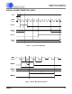
• MCLK = 2.048 MHz
• INR± Internal Input Capacitor = 20 pF
• Impedance = [1 / (2.048 MHz * 20 pF)] = 24 kΩ.