
Manual


32 DS626F5
CS5366
5. REGISTER MAP
In Control Port Mode, the bits in these registers are used to control all of the programmable features of the ADC. All
registers above 0Ah are RESERVED.
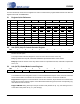
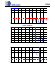
5.1 Register Quick Reference
5.2 00h (REVI) Chip ID Code & Revision Register
Default: See description
The Chip ID Code & Revision Register is used to store the ID and revision of the chip.
Bits[7:4] contain the chip ID, where the CS5366 is represented with a value of 0x6.
Bits[3:0] contain the revision of the chip, where revision A is represented as 0x0, revision B is represented
as 0x1, etc.
5.3 01h (GCTL) Global Mode Control Register
Default: 0x00
The Global Mode Control Register is used to control the Master/Slave Speed modes, the serial audio data
format and the Master clock dividers for all channels. It also contains a Control Port enable bit.
Bit[7] CP-EN manages the Control Port Mode. Until this bit is asserted, all pins behave as if in Stand-Alone
Mode. When this bit is asserted, all pins used in Stand-Alone Mode are ignored, and the corresponding reg-
ister values become functional.
Bit[6] CLKMODE Setting this bit puts the part in 384X mode (divides XTI by 1.5), and clearing the bit in-
vokes 256X mode (divide XTI by 1.0 - pass through).
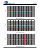
Adr Name76543210
00 REVI CHIP-ID[3:0] REVISION[3:0]
01 GCTL CP-EN CLKMODE MDIV[1:0] DIF[1:0] MODE[1:0]
02 OVFL RESERVED RESERVED OVFL6 OVFL5 OVFL4 OVFL3 OVFL2 OVFL1
03 OVFM RESERVED RESERVED OVFM6 OVFM5 OVFM4 OVFM3 OVFM2 OVFM1
04 HPF RESERVED RESERVED HPF6 HPF5 HPF4 HPF3 HPF2 HPF1
05 RESERVED - - - - - - - -
06 PDNE RESERVED PDN-BG PDN-OSC RESERVED PDN65 PDN43 PDN21
07 RESERVED - - - - - - - -
08 MUTE RESERVED RESERVED MUTE6 MUTE5 MUTE4 MUTE3 MUTE2 MUTE1
09 RESERVED - - - - - - - -
0A SDEN RESERVED RESERVED SDEN3
SDEN2 SDEN1
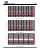
R/W76543210
R CHIP-ID[3:0] REVISION[3:0]
R/W76543210
R/W CP-EN CLKMODE MDIV[1:0] DIF[1:0] MODE[1:0]