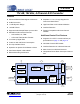
CS5364 114 dB, 192 kHz, 4-Channel A/D Converter Features Advanced Multi-bit Delta-Sigma Architecture 24-Bit Conversion Separate 1.
CS5364 Description The CS5364 is a complete 4-channel analog-to-digital converter for digital audio systems. It performs sampling, analog-to-digital conversion, and anti-alias filtering, generating 24-bit values for all 4-channel inputs in serial form at sample rates up to 216 kHz per channel. The CS5364 uses a 5th-order, multi-bit delta sigma modulator followed by low latency digital filtering and decimation, which removes the need for an external anti-aliasing filter.
CS5364 TABLE OF CONTENTS 1. PIN DESCRIPTION ................................................................................................................................. 6 2. TYPICAL CONNECTION DIAGRAM ..................................................................................................... 9 3. CHARACTERISTICS AND SPECIFICATIONS .................................................................................... 10 RECOMMENDED OPERATING CONDITIONS ...........................................
CS5364 5.3 01h (GCTL) Global Mode Control Register ................................................................................... 32 5.4 02h (OVFL) Overflow Status Register ........................................................................................... 33 5.5 03h (OVFM) Overflow Mask Register ............................................................................................ 33 5.6 04h (HPF) High-Pass Filter Register .................................................................
CS5364 LIST OF TABLES Table 1. Power Supply Pin Definitions ...................................................................................................... 19 Table 2. DIF1 and DIF0 Pin Settings ........................................................................................................ 23 Table 3. M1 and M0 Settings .................................................................................................................... 23 Table 4.
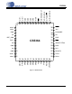
CS5364 DIF1/AD1/CDIN DIF0/AD0/CS M1/SCL/CCLK M0/SDA/CDOUT RST MDIV GND GND GND GND AIN1+ AIN1- 1. PIN DESCRIPTION 48 47 46 45 44 43 42 41 40 39 38 37 AIN2+ 1 36 OVFL AIN2- 2 VLC GND 3 VA 4 35 34 33 REF_GND 5 FILT+ 6 VQ GND 7 8 VA CLKMODE VD 32 31 GND 30 SDOUT1/TDM 29 GND 9 28 VLS GND 10 27 SDOUT2 AIN4+ 11 12 26 25 TSTO AIN4- CS5364 TDM SCLK LRCK/FS MCLK XTO XTI VX GND GND GND GND GND AIN3- AIN3+ 13 14 15 16 17 18 19 20 21 22 23 24 Figure 1.
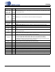
CS5364 Pin Name Pin # Pin Description AIN2+, AIN2AIN4+, AIN4AIN3+, AIN3AIN1+, AIN1- 1,2 11,12 13,14 47,48 Differential Analog (Inputs) - Audio signals are presented differently to the delta sigma modulators via the AIN+/- pins. GND 3,8 10,15 16,17 18,19 29,32 43,44 45,46 Ground (Input) - Ground reference. Must be connected to analog ground. VA 4,9 Analog Power (Input) - Positive power supply for the analog section. REF_GND 5 Reference Ground (Input) - For the internal sampling circuits.
CS5364 Stand-Alone Mode CLKMODE 34 CLKMODE (Input) - Setting this pin HIGH places a divide-by-1.5 circuit in the MCLK path to the core device circuitry. DIF1 DIF0 37 38 DIF1, DIF0 (Input) - Sets the serial audio interface format. M1 M0 39 40 Mode Selection (Input) - Determines the operational mode of the device. MDIV 42 MCLK Divider (Input) - Setting this pin HIGH places a divide-by-2 circuit in the MCLK path to the core device circuitry.
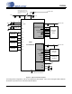
CS5364 2. TYPICAL CONNECTION DIAGRAM Resistor may only be used if VD is derived from VA. If used, do not drive any other logic from VD. +5V + 0.01 F 1 F 5.1 4, 9 VA 6 220 F 1F + + 0.1 F 5 7 0.1 F Channel 1 Analog Input Buffer Channel 2 Analog Input Buffer Channel 3 Analog Input Buffer Channel 4 Analog Input Buffer 8 47 48 1 2 13 14 11 12 + +5V to 3.3V 1 F 0.
CS5364 3. CHARACTERISTICS AND SPECIFICATIONS RECOMMENDED OPERATING CONDITIONS GND = 0 V, all voltages with respect to 0 V. Parameter DC Power Supplies: Symbol Min Typ Max Unit Positive Analog Positive Crystal Positive Digital Positive Serial Logic Positive Control Logic VA VX VD VLS VLC 4.75 4.75 3.14 1.711 1.71 5.0 5.0 3.3 3.3 3.3 5.25 V (-CQZ) (-DQZ) TAC TAA -40 -40 - 85 105 °C Ambient Operating Temperature 1. TDM Quad-Speed Mode specified to operate correctly at VLS 3.14 V.
CS5364 DC POWER MCLK = 12.288 MHz; Master Mode. GND = 0 V. Parameter Symbol Min Typ Max Unit VA = 5 V VX = 5 V VD = 5 V VD = 3.3 V VLS, VLC = 5 V VLS, VLC = 3.3 V IA IX ID ID IL IL - 51 4 44 25 3 1 56 8 48 28 4 2 mA mA mA mA mA mA VA = 5 V VLS, VLC,VD = 5 V IA ID - 50 500 - A A All Supplies = 5 V VA = 5 V, VD = VLS = VLC = 3.3 V - - 510 360 2.
CS5364 ANALOG CHARACTERISTICS (COMMERCIAL) Test Conditions (unless otherwise specified). VA = 5 V, VD = VLS = VLC 3.3 V, and TA = 25° C. Full-scale input sine wave. Measurement Bandwidth is 10 Hz to 20 kHz. Parameter Min Typ Max Unit 108 105 114 111 - dB - -105 -91 -51 -99 -45 dB 108 105 - 114 111 108 - dB - -105 -91 -51 -102 -99 -45 - dB 108 105 - 114 111 108 - dB - -105 -91 -51 -102 -99 -45 - dB - 110 - dB Interchannel Gain Mismatch - 0.
CS5364 ANALOG PERFORMANCE (AUTOMOTIVE) Test Conditions (unless otherwise specified). VA = 5.25 to 4.75 V, VD = 5.25 to 3.14 V, VLS = VLC = 5.25 to 1.71 V and TA = -40° to +85° C. Full-scale input sine wave. Measurement Bandwidth is 10 Hz to 20 kHz.
CS5364 DIGITAL FILTER CHARACTERISTICS Parameter Symbol Min Typ Max Unit Single-Speed Mode (2 kHz to 54 kHz sample rates) 0 0.47 Fs Passband Ripple Passband (Note 1) (-0.1 dB) -0.035 0.035 dB Stopband (Note 1) 0.58 Stopband Attenuation - -95 Total Group Delay (Fs = Output Sample Rate) tgd - Fs - 12/Fs dB s Double-Speed Mode (54 kHz to 108 kHz sample rates) Passband (Note 1) (-0.1 dB) 0 Passband Ripple -0.035 Stopband (Note 1) 0.
CS5364 SERIAL AUDIO INTERFACE - I²S/LJ TIMING The serial audio port is a three-pin interface consisting of SCLK, LRCK and SDOUT. Logic "0" = GND = 0 V; Logic "1" = VLS; CL = 20 pF, timing threshold is 50% of VLS. Parameter Symbol Min Typ Max Unit - 2 54 108 - 54 108 216 kHz 1/(64*216 kHz) (CLKMODE = 0)(Note 2) (CLKMODE = 1)(Note 2) tPERIOD tHIGH tHIGH 64*Fs 72.
CS5364 SERIAL AUDIO INTERFACE - TDM TIMING The serial audio port is a three-pin interface consisting of SCLK, LRCK and SDOUT. Logic "0" = GND = 0 V; Logic "1" = VLS; CL = 20 pF, timing threshold is 50% of VLS.
CS5364 SWITCHING SPECIFICATIONS - CONTROL PORT - I²C TIMING Inputs: Logic 0 = DGND, Logic 1 = VLC, SDA CL = 30 pF Symbol Min Max Unit SCL Clock Frequency Parameter fscl - 100 kHz RST Rising Edge to Start tirs 600 ns Bus Free Time Between Transmissions tbuf 4.7 µs Start Condition Hold Time (prior to first clock pulse) thdst 4.0 Clock Low time tlow 4.7 Clock High Time thigh 4.0 Setup Time for Repeated Start Condition tsust 4.
CS5364 SWITCHING SPECIFICATIONS - CONTROL PORT - SPI TIMING Inputs: Logic 0 = DGND, Logic 1 = VLC, CDOUT CL = 30 pF Parameter Symbol Min Max Units CCLK Clock Frequency fsck 0 6.0 MHz RST Rising Edge to CS Falling tsrs 20 CS Falling to CCLK Edge tcss 20 CS High Time Between Transmissions tcsh 1.
CS5364 4. APPLICATIONS 4.1 Power CS5364 features five independent power pins that power various functional blocks within the device and allow for convenient interfacing to other devices. Table 1 shows what portion of the device is powered from each supply pin. Please refer to “Recommended Operating Conditions” on page 10 for the valid range of each power supply pin. The power supplied to each power pin can be independent of the power supplied to any other pin.
CS5364 4.3 Master Clock Source The CS5364 requires a Master Clock that can come from one of two sources: an on-chip crystal oscillator driver or an externally generated clock. 4.3.1 On-Chip Crystal Oscillator Driver When using the on-board crystal oscillator driver, the XTI pin (pin 21) is the input for the Master Clock (MCLK) to the device. The XTO pin (pin 22) must not be used to drive anything other than the oscillator tank circuitry.
CS5364 4.4 Master and Slave Operation CS5364 operation depends on two clocks that are synchronously derived from MCLK: SCLK and LRCK/FS. See Section 4.5 on page 22 for a detailed description of SCLK and LRCK/FS. The CS5364 can operate as either clock master or clock slave with respect to SCLK and LRCK/FS. In Master Mode, the CS5364 derives SCLK and LRCK/FS synchronously from MCLK and outputs the derived clocks on the SCLK pin (pin 25) and the LRCK/FS pin (pin 24), respectively.
CS5364 4.5 Serial Audio Interface (SAI) Format The SAI port consists of two timing pins (SCLK, LRCK/FS) and four audio data output pins (SDOUT1/TDM, SDOUT2, SDOUT3/TDM and SDOUT4). The CS5364 output is serial data in I²S, Left-Justified (LJ), or Time Division Multiplexed (TDM) digital audio interface formats. These formats are available to the user in both Stand-Alone Mode and Control Port Mode. 4.5.1 I²S and LJ Format The I²S and LJ formats are both two-channel protocols.
CS5364 4.5.2 TDM Format In TDM Mode, all four channels of audio data are serially clocked out during a single Frame Sync (FS) cycle, as shown in Figure 12. The rising edge of FS signifies the start of a new TDM frame cycle. Each channel slot occupies 32 SCLK cycles, with the data left justified and with MSB first. TDM output data should be latched on the rising edge of SCLK within time specified under ”Serial Audio Interface - TDM Timing” section on page 16.
CS5364 4.6.3 Master Mode Clock Dividers Figure 13 shows the configuration of the MCLK dividers and the sample rate dividers for Master Mode, including the significance of each MCLK divider pin (in Stand-Alone Mode) or bit (in Control Port Mode). SAMPLE RATE DIVIDERS MCLK DIVIDERS MCLK pin bit 0/1 0/1 ÷1 ÷1 ÷1 ÷ 1.
CS5364 4.7 Master and Slave Clock Frequencies Tables 4 through 12 show the clock speeds for sample rates of 48 kHz, 96 kHz and 192 kHz. The MCLK/LRCK ratio should be kept at a constant value during each mode. In Master Mode, the device outputs the frequencies shown. In Slave Mode, the SCLK/LRCK ratio can be set according to design preference. However, device performance is guaranteed only when using the ratios shown in the tables.
CS5364 TDM MASTER DSM Fs = 96 kHz MCLK Divider 4 3 2 - - MCLK (MHz) 49.152 36.864 24.567 - - SCLK (MHz) 24.576 24.576 24.576 - - MCLK/FS Ratio 512 384 256 - - SCLK/FS Ratio 256 256 256 - - Table 9. Frequencies for 96 kHz Sample Rate using TDM TDM SLAVE DSM Fs = 96 kHz MCLK Divider 4 3 2 1.5 1 MCLK (MHz) 49.152 36.864 24.567 18.384 12.288 SCLK (MHz) 24.576 24.576 24.576 24.576 24.
CS5364 4.8 Reset The device should be held in reset until power is applied and all incoming clocks are stable and valid. Upon de-assertion of RST, the state of the configuration pins is latched, the state machine begins, and the device starts sending audio output data a maximum of 524288 MCLK cycles after the release of RST.
CS5364 4.10 Analog Connections The analog modulator samples the input at half of the internal Master Clock frequency, or 6.144 MHz nominally. The digital filter will reject signals within the stopband of the filter. However, there is no rejection of input signals that are at (N X 6.144 MHz) the digital passband frequency, where n=0,1,2.... Refer to Figure 15, which shows the suggested filter that will attenuate any noise energy at 6.
CS5364 4.11 Optimizing Performance in TDM Mode Noise Management is a design technique that is utilized in the majority of audio A/D converters. Noise management is relatively simple conceptually. The goal of noise management is to interleave the on-chip digital activity with the analog sampling processes to ensure that the noise generated by the digital activity is minimized (ideally non-existant) when the analog sampling occurs.
CS5364 4.13 Control Port Operation The Control Port is used to read and write the internal device registers. It supports two industry standard formats, I²C and SPI. The part is in I²C format by default. SPI Mode is selected if there is ever a high-to-low transition on the AD0/CS pin after the RST pin has been restored high. In Control Port Mode, all features of the CS5364 are available. Four multi-use configuration pins become software pins that support the I²C or SPI bus protocol.
CS5364 4.13.2 I²C Mode In I²C Mode, SDA is a bidirectional data line. Data is clocked into and out of the part by the clock, SCL. There is no CS pin. Pins AD0 and AD1 form the two least-significant bits of the chip address and should be connected through a resistor to VLC or DGND, as desired. The state of the pins is latched when the CS5364 is being released from RST. A Start condition is defined as a falling transition of SDA while SCL is high.
CS5364 5. REGISTER MAP In Control Port Mode, the bits in these registers are used to control all of the programmable features of the ADC. All registers above 0Ah are RESERVED. 5.
CS5364 Bits[5:4] MDIV[1:0] Each bit selects an XTI divider. When either bit is low, an XTI divide-by-1 function is selected. When either bit is HIGH, an XTI divide-by-2 function is selected. With both bits HIGH, XTI is divided by 4. The table below shows the composite XTI division using both CLKMODE and MDIV[1:0]. CLKMODE,MDIV[1],MDIV[0] 000 100 001 or 010 101 or 110 011 111 DESCRIPTION Divide-by-1 Divide-by-1.
CS5364 5.6 04h (HPF) High-Pass Filter Register R/W R/W 7 6 5 4 RESERVED RESERVED RESERVED RESERVED 3 2 1 0 HPF4 HPF3 HPF2 HPF1 Default: 0x00, all high-pass filters enabled. The High-Pass Filter Register is used to enable or disable a high-pass filter that exists for each channel. These filters are used to perform DC offset calibration, a procedure that is detailed in “DC Offset Control” on page 29. 5.7 05h Reserved R/W RESERVED 5.
CS5364 5.11 09h Reserved R/W RESERVED 5.12 7 - 6 - 5 - 4 - 3 - 2 - 1 - 0 - 1 SDEN2 0 SDEN1 0Ah (SDEN) SDOUT Enable Control Register R/W R/W 7 6 5 RESERVED 4 3 2 RESERVED RESERVED Default: 0x00, all SDOUT pins enabled. The SDOUT Enable Control Register is used to tri-state the serial audio data output pins. Each bit, when set, tri-states the associated SDOUT pin.
CS5364 6. FILTER PLOTS 0.1 0.08 0.06 Amplitude (dB) 0.04 0.02 0 −0.02 −0.04 −0.06 −0.08 −0.1 0 0.05 0.1 0.15 0.2 0.25 0.3 Frequency (normalized to Fs) 0.35 0.4 0.45 0.5 0.35 0.4 0.45 0.5 Figure 19. SSM Passband 0.1 0.08 0.06 Amplitude (dB) 0.04 0.02 0 −0.02 −0.04 −0.06 −0.08 −0.1 0 0.05 0.1 0.15 0.2 0.25 0.3 Frequency (normalized to Fs) Figure 20. DSM Passband 0.1 0.08 0.06 Amplitude (dB) 0.04 0.02 0 −0.02 −0.04 −0.06 −0.08 −0.1 0 0.05 0.1 0.15 Frequency (normalized to Fs) 0.
CS5364 0 −20 Amplitude (dB) −40 −60 −80 −100 −120 −140 0 0.1 0.2 0.3 0.4 0.5 0.6 Frequency (normalized to Fs) 0.7 0.8 0.9 1 0.7 0.8 0.9 1 0.7 0.8 0.9 1 Figure 22. SSM Stopband 0 −20 Amplitude (dB) −40 −60 −80 −100 −120 −140 0 0.1 0.2 0.3 0.4 0.5 0.6 Frequency (normalized to Fs) Figure 23. DSM Stopband 0 −20 Amplitude (dB) −40 −60 −80 −100 −120 0 0.1 0.2 0.3 0.4 0.5 0.6 Frequency (normalized to Fs) Figure 24.
CS5364 0 −0.2 −0.4 Amplitude (dB) −0.6 −0.8 −1 −1.2 −1.4 −1.6 −1.8 −2 0.4 0.42 0.44 0.46 0.48 0.5 0.52 Frequency (normalized to Fs) 0.54 0.56 0.58 0.6 0.54 0.56 0.58 0.6 0.34 0.36 0.38 0.4 Figure 25. SSM -1 dB Cutoff 0 −0.2 −0.4 Amplitude (dB) −0.6 −0.8 −1 −1.2 −1.4 −1.6 −1.8 −2 0.4 0.42 0.44 0.46 0.48 0.5 0.52 Frequency (normalized to Fs) Figure 26. DSM -1 dB Cutoff 0 −0.2 −0.4 Amplitude (dB) −0.6 −0.8 −1 −1.2 −1.4 −1.6 −1.8 −2 0.2 0.22 0.24 0.26 0.28 0.3 0.
CS5364 7. PARAMETER DEFINITIONS Dynamic Range The ratio of the rms value of the signal to the rms sum of all other spectral components over the specified bandwidth. Dynamic Range is a signal-to-noise ratio measurement over the specified bandwidth made with a -60 dBFS signal. 60 dB is added to resulting measurement to refer the measurement to full scale. This technique ensures that the distortion components are below the noise level and do not affect the measurement.
CS5364 8. PACKAGE DIMENSIONS 48L LQFP PACKAGE DRAWING E E1 D D1 1 e B A A1 L DIM A A1 B D D1 E E1 e* L MIN --0.002 0.007 0.343 0.272 0.343 0.272 0.016 0.018 0.000° INCHES NOM 0.055 0.004 0.009 0.354 0.28 0.354 0.28 0.020 0.24 4° MAX 0.063 0.006 0.011 0.366 0.280 0.366 0.280 0.024 0.030 7.000° MIN --0.05 0.17 8.70 6.90 8.70 6.90 0.40 0.45 0.00° MILLIMETERS NOM 1.40 0.10 0.22 9.0 BSC 7.0 BSC 9.0 BSC 7.0 BSC 0.50 BSC 0.60 4° MAX 1.60 0.15 0.27 9.30 7.10 9.30 7.10 0.60 0.75 7.
CS5364 9. ORDERING INFORMATION Product Description Package Pb-Free CS5364 114 dB, 192 kHz, 4-channel A/D Converter 48-pin LQFP YES CDB5364 Evaluation Board for CS5364 Grade Temp Range Container Order # Tray CS5364-CQZ Commercial -40°C to +85°C Tape & Reel CS5364-CQZR Tray CS5364-DQZ Automotive -40°C to +105°C Tape & Reel CS5364-DQZR CDB5364 10.REVISION HISTORY Revision Changes F1 Initial release.
CS5364 Contacting Cirrus Logic Support For all product questions and inquiries, contact a Cirrus Logic Sales Representative. To find the one nearest you, go to www.cirrus.com. IMPORTANT NOTICE Cirrus Logic, Inc. and its subsidiaries ("Cirrus") believe that the information contained in this document is accurate and reliable. However, the information is subject to change without notice and is provided "AS IS" without warranty of any kind (express or implied).