
Manual

DS861PP3 3
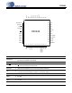
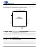
CS5346
7.6.1 Channel B PGA Gain (Bits 5:0) ............................................................................................. 30
7.7 Channel A PGA Control - Address 08h .......................................................................................... 31
7.7.1 Channel A PGA Gain (Bits 5:0) ............................................................................................. 31
7.8 ADC Input Control - Address 09h ................................................................................................... 31
7.8.1 PGA Soft Ramp or Zero Cross Enable (Bits 4:3) .................................................................. 31
7.8.2 Analog Input Selection (Bits 2:0) ........................................................................................... 32
7.9 Active Level Control - Address 0Ch ................................................................................................ 32
7.9.1 Active High/ Low (Bit 0) ......................................................................................................... 32
7.10 Status - Address 0Dh ................................................................................................................... 32
7.10.1 Clock Error (Bit 3) ................................................................................................................ 33
7.10.2 Overflow (Bit 1) .................................................................................................................... 33
7.10.3 Underflow (Bit 0) .................................................................................................................. 33
7.11 Status Mask - Address 0Eh .......................................................................................................... 33
7.12 Status Mode MSB - Address 0Fh ................................................................................................. 33
7.13 Status Mode LSB - Address 10h .................................................................................................. 33
8. PARAMETER DEFINITIONS ................................................................................................................ 34
9. FILTER PLOTS .................................................................................................................................. 35
10. PACKAGE DIMENSIONS .................................................................................................................. 37
11. THERMAL CHARACTERISTICS AND SPECIFICATIONS .............................................................. 37
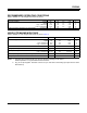
12. ORDERING INFORMATION ......................................................................................................... 38
13. REVISION HISTORY .......................................................................................................................... 38
LIST OF FIGURES
Figure 1.Master Mode Serial Audio Port Timing ....................................................................................... 15
Figure 2.Slave Mode Serial Audio Port Timing ......................................................................................... 15
Figure 3.Format 0, 24-Bit Data Left-Justified ............................................................................................ 15
Figure 4.Format 1, 24-Bit Data I²S ............................................................................................................ 15
Figure 5.Control Port Timing - I²C Format ................................................................................................. 16
Figure 6.Control Port Timing - SPI Format ................................................................................................ 17
Figure 7.Typical Connection Diagram ....................................................................................................... 18
Figure 8.Master Mode Clocking ................................................................................................................ 20
Figure 9.Analog Input Architecture ............................................................................................................ 21
Figure 10.CS5346 PGA ............................................................................................................................ 22
Figure 11.1 V
RMS
Input Circuit .................................................................................................................. 22
Figure 12.1 V
RMS
Input Circuit with RF Filtering ....................................................................................... 22
Figure 13.2 V
RMS
Input Circuit .................................................................................................................. 22
Figure 14.Control Port Timing in SPI Mode .............................................................................................. 24
Figure 15.Control Port Timing, I²C Write ................................................................................................... 24
Figure 16.Control Port Timing, I²C Read ................................................................................................... 25
Figure 17.Single-Speed Stopband Rejection ............................................................................................ 35
Figure 18.Single-Speed Stopband Rejection ............................................................................................ 35
Figure 19.Single-Speed Transition Band (Detail) ...................................................................................... 35
Figure 20.Single-Speed Passband Ripple ................................................................................................ 35
Figure 21.Double-Speed Stopband Rejection ........................................................................................... 35
Figure 22.Double-Speed Stopband Rejection ........................................................................................... 35
Figure 23.Double-Speed Transition Band (Detail) .................................................................................... 36
Figure 24.Double-Speed Passband Ripple ............................................................................................... 36
Figure 25.Quad-Speed Stopband Rejection ............................................................................................. 36
Figure 26.Quad-Speed Stopband Rejection ............................................................................................. 36
Figure 27.Quad-Speed Transition Band (Detail) ....................................................................................... 36
Figure 28.Quad-Speed Passband Ripple ................................................................................................. 36