
Manual

DS861PP3 17
CS5346
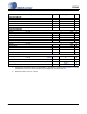
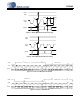
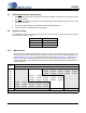
SWITCHING CHARACTERISTICS - CONTROL PORT - SPI FORMAT
Inputs: Logic 0 = DGND = AGND = 0 V, Logic 1 = VLC, C
L
=30pF.
14. Data must be held for sufficient time to bridge the transition time of CCLK.
15. For f
sck
<1 MHz.
Parameter Symbol Min Max Units
CCLK Clock Frequency f
sck
-6.0MHz
RST
Rising Edge to CS Falling t
srs
500 - ns
CS High Time Between Transmissions t
csh
1.0 - s
CS Falling to CCLK Edge t
css
20 - ns
CCLK Low Time t
scl
66 - ns
CCLK High Time t
sch
66 - ns
CDIN to CCLK Rising Setup Time t
dsu
40 - ns
CCLK Rising to DATA Hold Time (Note 14) t
dh
15 - ns
CCLK Falling to CDOUT Stable t
pd
-50ns
Rise Time of CDOUT t
r1
-25ns
Fall Time of CDOUT t
f1
-25ns
Rise Time of CCLK and CDIN (Note 15) t
r2
- 100 ns
Fall Time of CCLK and CDIN (Note 15) t
f2
- 100 ns
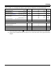
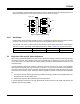
t
r2
t
f2
t
dsu
t
dh
t
sch
t
scl
CS
CCLK
CDIN
t
css
t
pd
CDOUT
t
csh
RST
t
srs
Figure 6. Control Port Timing - SPI Format