
User Manual


DS658F4 5
CS5345
1. PIN DESCRIPTIONS
Pin Name # Pin Description
SDA/CDOUT 1
Serial Control Dat a (Input/Output) - SDA is a data I/O in I²C
®
Mode. CDOUT is the output data line for
the control port interface in SPI
TM
Mode.
SCL/CCLK 2 Serial Control Port Clock (Input) - Serial clock for the serial control port.
AD0/CS
3
Address Bit 0 (I²C) / Control Port Chip Select (SPI) (Input) - AD0 is a chip address pin in I²C Mode;
CS
is the chip-select signal for SPI format.
AD1/CDIN 4
Address Bit 1 (I²C) / Serial Control Data Input (SPI) (Input) - AD1 is a chip address pin in I²C Mode;
CDIN is the input data line for the control port interface in SPI Mode.
VLC 5
Control Port Power (Input) - Determines the required signal level for the control port interface. Refer
to the Recommended Operating Conditions for appropriate voltages.
RESET
6 Reset (Input) - The device enters a low-power mode when this pin is driven low.
AIN3A
AIN3B
7
8
Stereo Analog Input 3 (Input) - The full-scale level is specified in the ADC Analog Characteristics
specification table.
AIN2A
AIN2B
9
10
Stereo Analog Input 2 (Input) - The full-scale level is specified in the ADC Analog Characteristics
specification table.
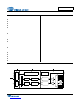
1
2
3
4
5
6
7
8
9
10
11
12
13 14 15 16 17 18 19 20 21 22 23 24
48 47 46 45 44 43 42 41 40 39 38 37
36
35
34
33
32
31
30
29
28
27
26
25
VLSSDA/CDOUT
AGND
OVFL
SCL/CCLK
AD0/CS
AD1/CDIN
VLC
RESET
AIN3A
AIN3B
AIN2A
AIN2B
AIN1A
AIN1B
VA
AFILTB
VQ
TSTO
FILT+
TSTO
AIN4A/MICIN1
AIN4B/MICIN2
AIN5A
AIN5B
AFILTA
TSTO
NC
NC
AGND
AGND
VA
PGAOUTB
PGAOUTA
AIN6B
AIN6A
MICBIAS
INT
VD
DGND
MCLK
LRCK
SCLK
SDOUT
NC
NC
NC
TSTI
CS5345