
User guide


5-2 Copyright 2013 Cirrus Logic, Inc. DS810UM6
SDRAM Controller
CS4953x4/CS4970x4 System Designer’s Guide
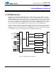
5.1.1 SDRAM Controller Interface
The physical interface of the SDRAM controller consists of 16 data pins (SD_DATA[15:0]), 13 address
pins (SD_ADDR[12:0]), 2 bank address pins (SD_BA[1:0]), and 9 control pins (SD_CS
, SD_WE,
SD_DQM1
, SD_DQM0, SD_CAS, SD_RAS, SD_CLKOUT, SD_CLKIN, SD_CLKEN). SD_CS is the
SDRAM chip select pin. The address and data pins are shared with the Flash interface. The CS4953x4/
CS4970x4 supports SDRAMs from 2 Mbytes to 64 Mbytes with various row, bank, and column
configurations. The size can be configured in the DynamicConfig0 register listed in Table 5-2. Timing
parameters of the SDRAM port can be configured to meet various SDRAM requirements as described in
Table 5-2. The default timing parameters have been chosen and tested to meet the requirements of Hynix
HY57V641620HG-H. By default, the SDRAM port is configured for 64 Mbits with 4 banks, 12 rows, and 8
columns with a RAS and CAS latency of 3.
Note:When connected to a 16 Mbit SDRAM, the CS4953x4/CS4970x4 uses only SD_BA0 for bank
selection.
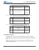
5.1.2 SDRAM Interface Signals
Table 5-1 shows the signal names, descriptions, and pin number of the signals associated with the
external SDRAM memory control port on the CS4953x4/CS4970x4 chip.
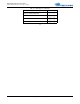
Table 5-1. SDRAM Interface Signals
Signal Name Signal Description
LQFP-144
Pin #
LQFP-128
Pin #
Pin Type
SD_CLKOUT
SDRAM clock output. This output is tri-stated when
SDRAM interface is not used.
51 80 Output
SD_CLKIN
SDRAM Clock input
Connects to trace from SDRAM device CLKIN pin.
52 81 Input
SD_CLKEN SDRAM Clock Enable Output 53 82 Output
SD_RAS SDRAM Row Address Strobe 80 109 Output
SD_CAS SDRAM Column Address Strobe 79 108 Output
SD_CS SDRAM Chip Select 81 110 Output
SD_DQM0 SDRAM Data Mask 0 28 57 Output
SD_DQM1 SDRAM Data Mask 1 50 79 Output
SD_WE SDRAM Write Enable 78 107 Output
SD_A0 SDRAM Address 0 72 102 Output
SD_A1 SDRAM Address 1 71 101 Output
SD_A2 SDRAM Address 2 70 99 Output
SD_A3 SDRAM Address 3 68 97 Output
SD_A4 SDRAM Address 4 67 96 Output
SD_A5 SDRAM Address 5 64 93 Output
SD_A6 SDRAM Address 6 62 91 Output
SD_A7 SDRAM Address 7 61 90 Output
SD_A8 SDRAM Address 8 59 88 Output
SD_A9 SDRAM Address 9 58 87 Output