
User guide


Digital Audio Input Port Description
CS4953x4/CS4970x4 System Designer’s Guide
DS810UM6 Copyright 2013 Cirrus Logic, Inc 3-7
3.4 Digital Audio Input Port Description
CS4953x4/CS4970x4 is capable of accepting DSD audio data directly. DSD data differs from PCM in that
audio is provided as a contiguous stream of 1’s and 0’s on a single line. There is no framing clock
(LRCLK), and there is only one channel per line. The CS4953x4/CS4970x4 supports internal conversion
of DSD data to PCM which can then be processed by the DSP.
The CS4953x4/CS4970x4 DSD port is designed to accept DSD audio data from up to 6 pins
simultaneously (6 channels total)
DSD features include:
• Six DSD Input Pins
• One Shared DSD_CLK for All Data Pins
• Supports 44.1 KHz and 88.2 KHz Sample Rates
3.4.1 DSD Pin Description
Table 3-7 shows the mnemonic and pin description of the pins associated with the DSD port on
CS4953x4/CS4970x4.
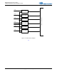
3.4.2 Supported DSD Functional Blocks
Figure 3-3 shows the functional block diagram of the features currently supported with the CS4953x4/
CS4970x4 DSD Port.
4
DAI1_LRCLK/SCLK - Slave
Compressed Data on
DAI_D0 and DAI_D0 to DAI_D4 enabled
0x81000025
0X0000D11F
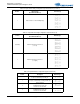
Table 3-7. DSDl Audio Input Port
Pin Name Pin Description
LQFP-144
Pin #
LQFP-128
Pin #
Pin Type
DSD_CLK
Bit clock used for latching the DSD audio data.
This clock is shared by DSD[5:0].
137 29 Input
DSD0 DSD Audio Input 0 135 27 Input
DSD1 DSD Audio Input 1 134 26 Input
DSD2 DSD Audio Input 2 132 24 Input
DSD3 DSD Audio Input 3 131 23 Input
DSD4 DSD Audio Input 4 138 34 Input
DSD5 DSD Audio Input 5 142 30 Input
Table 3-6. Input DAI Mode Configuration (Input Parameter D) (Continued)
D Value Description HEX Message