
User guide


DS810UM6 Copyright 2013 Cirrus Logic, Inc 2-19
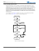
I2C Port
CS4953x4/CS4970x4 System Designer’s Guide
Figure 2-16. Sample Waveform for I
2
C Write Functional TIming
Note: The I2C Slave is always responsible for driving the ACK for the address byte.
Figure 2-17. Sample Waveform for I
2
C Read Functional TIming
Note:
1. The I
2
C Slave drives the ACK for the address byte.
2. The I
2
C Master is responsible for controlling ACK during I
2
C reads. In general, the receiver in an I
2
C transaction is responsible for providing ACK.
3. SCP1_IRQ
remains low until the rising edge of the clock for the last bit of the last byte read from the I
2
C Slave.
4. A NACK
is sent by the Master after the last byte to indicate the end of the read cycle. This must be followed with an I
2
C Stop condition or I
2
C Repeated-
Start condition.
5. If there are more data words to read, IRQ will fall at the rising edge of CLK for the NACK. Otherwise, IRQ remains high until an I
2
C Stop condition or an I
2
C
Repeated-Start condition occurs.
Start
SCP1_CLK
SCP1_SDA
Data Byte 3 (MSB)
Stop
7-bit Address
R
/W
AC
K
AC
K
Data Byte 2
AC
K
Data Byte 1
AC
K
Data Byte 0 (LSB)
ACK
M S M S M S M S M S M
Start
SCP1_CLK
SCP1_SDA
Data Byte 3 (MSB)
Stop
7-bit Address
R
/W
A
C
K
ACK
Data Byte 2
AC
K
Data Byte 1
A
C
K
Data Byte 0 (LSB)
SCP1_IRQ#
N
ACK
M S S M S M S M S M M
M = Master Drives SDA
S = Slave Drives SDA