
User guide


I2C Port
CS4953x4/CS4970x4 System Designer’s Guide
DS810UM6 Copyright 2013 Cirrus Logic, Inc 2-9
2.4.3.5 SCP1_IRQ Behavior
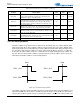
The SCP1_IRQ signal is not part of the SPI protocol, but is provided so that the Slave can signal that it
has data to be read. A high-to-low transition on SCP1_IRQ
indicates to the Master that the Slave has data
to be read. When a Master detects a high-to-low transition on SCP1_IRQ
, it should send a Start condition
and begin reading data from the Slave.
SCP1_IRQ
is guaranteed to remain low (once it has gone low), until the rising edge of SCP1_CLK for the
last bit of the last byte to be transferred out of the CS4953x4/CS4970x4. If there is no more data to be
transferred, SCP1_IRQ
will go high at this point. After going high, SCP1_IRQ is guaranteed to stay high
until the rising edge of SCP1_CS
.
This end-of-transfer condition signals the Master to end the read transaction by clocking the last data bit
out of the CS4953x4/CS4970x4 and then driving the CS4953x4/CS4970x4 SCP1_CS
line high to signal
that the read sequence is over. If SCP1_IRQ
is still low after the rising edge of SCP1_CLK on the last data
bit of the current byte, the Master should continue reading data from the serial control port. It should be
noted that all data should be read out of the serial control port during one cycle or a loss of data will occur.
In other words, all data should be read out of the chip until SCP1_IRQ
signals the last byte by going high
as described above.
2.5 I
2
C Port
The CS4953x4/CS4970x4 I
2
C bus has been developed for 8-bit digital control applications, such as those
requiring microcontrollers. The I
2
C bus interface is a bidirectional serial port that uses 2 lines (data and
clock) for data transmission and reception with software-addressable external devices. Each external
device interfaced to the CS4953x4/CS4970x4 I
2
C port has the ability to communicate directly with the
other devices and is assigned a unique address whether it is a CPU, memory, or some other device. A
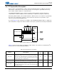
block diagram of the CS4953x4/CS4970x4 I
2
C Serial Control Port is provided in Figure 2-7.
Figure 2-7. Serial Control Port Internal Block Diagram
I2C Control /
Clocking
SCP1_BSY
SCP1_IRQ
LSB (Byte 0)Byte 1Byte2MSB (Byte 3)
LSB (Byte 0)Byte 1Byte2MSB (Byte 3)
MSB (Byte 3)Byte 2Byte1LSB (Byte 0)
MSB (Byte 3)Byte 2Byte1LSB (Byte 0)
7 6 5 4 3 2 1 0
Internal Bus
SCP1_SDA
SCP1_CLK
EN
EN