
User guide


1-6 Copyright 2013 Cirrus Logic, Inc. DS810UM6
Booting the DSP in Master Boot Mode
CS4953x4/CS4970x4 System Designer’s Guide
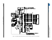
The typical connection diagram in Figure 1-2 and Figure 1-3 is shown with a microcontroller controlling
the DSP in SPI mode. Details of the SPI protocol can be found in Section 2.4, "SPI Port" on page 2-1. An
external SDRAM is also shown in Figure 1-2 and Figure 1-3 The external SDRAM is required for systems
that require HD decoders. Care must be taken when routing this interface. This interface will run at 150
MHz during normal operation. Details of the SDRAM interface can be found in Chapter 5, "External
Memory Interfaces".
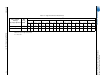
An 2x10 header J1 is shown in Figure 1-2 and Figure 1-3. This Header is optional but highly
recommended. The Header performs three functions:
1. Allows a blank SPI Flash to be programmed with the Cirrus Logic CDB USB Master board
2. Allows a user to use the Cirrus Logic DSP Composer development tool on an end product.
3. Allows a Cirrus Logic representative to easily debug an end system.
A SPDIF_RX, HDMI_RX and ADCs are shown in Figure 1-2 and Figure 1-3. These outputs of these
devices are connected to inputs of the DSP. These devices provide data to the DAI port of the DSP.
Details of the DAI port are described in Chapter 3, "Audio Input Interfaces".
DACs are shown in Figure 1-2. The output of the DSP is connected to the input of the DACs. The DSP
has a total of 8 output lines and can generate up to 16 channels of audio. Details of the DAO port are
described in Chapter 4.
Special attention must be paid to configuring the clocks in an AVR system. As seen in Figure 1-2, the input
and output clock domains are independent but all synchronous to MCLK. The DSP is a Slave to all clocks
on the input side and hence the S/PDIF_RX, HDMI_RX and ADCs must be configured to be the Master to
MCLK, SCLK, and LRCLK for the DSP. On the output side, the DSP is a Slave to MCLK and a Master to
SCLK and LRCK. The frequency of the SCLK and LRCLK can be configured at design time in DSP
Condenser. Refer to Chapter 8, "DSP Condenser"" for more details.
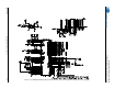
1.3.1 Performing a Master Boot
When the DSP is connected as shown in Figure 1-2 and Figure 1-3, the boot procedure to boot the DSP
is described in Figure 1-4.
Pseudocode and flowcharts will be used to describe each of these boot procedures in detail. The flow
charts use the following messages:
• Read_* – Read from CS4953x4/CS4970x4
Please note that * above can be replaced by SPI
™
or I
2
C. The system designer should also refer to the
control port sections of this document in Chapter 2, "Serial Communication Mode"", for the details of
writing to and reading from the CS4953x4/CS4970x4.