
User guide


DS810UM6 Copyright 2013 Cirrus Logic P-24
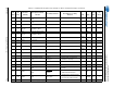
CS4953x4 Pin Assignments
CS4953x4/CS4970x4 System Designer’s Guide
99 126 GPIO35
General Purpose Input/
Output
SCP1_CLK
SPI/I
2
C Control Port Clock
3.3V (5V
tol)
BiDir/OD IN Y
100 - GPIO36
General Purpose Input/
Output
SCP1_IRQ
Serial Control Port Data Ready
Interrupt Request
3.3V (5V
tol)
BiDir/OD IN Y
101 127 GNDD6 Core ground 0V PWR
102 - GPIO37
General Purpose Input/
Output
1. SCP1_BSY
2. PCP_BSY
1. Serial Control Port 1 Input Busy
2. Parallel Control Port Input Busy
3.3V (5V
tol)
BiDir/OD IN Y
- 128 GPIO37
General Purpose Input/
Output
1. SCP1_BSY
1. Serial Control Port 1 Input Busy
3.3V (5V
tol)
BiDir/OD IN Y
103 - GPIO38
General Purpose Input/
Output
1. PCP_WR
2. PCP_DS
3. SCP2_CLK
1. Parallel Port Write Select (Intel
Mode)
2. Parallel Port Data Strobe (Motorola
and Multiplexed Mode)
3. SPI/I
2
C Control Port Clock
3.3V (5V
tol)
BiDir/OD IN Y
-1GPIO38
General Purpose Input/
Output
1. SCP2_CLK
1. SPI/I
2
C Control Port Clock
3.3V (5V
tol)
BiDir/OD IN Y
104 - GPIO39
General Purpose Input/
Output
1. PCP_CS
2. SCP2_CS
1. Parallel Port Chip Select (Intel/
Motorola/Multiplexed Mode)
2. SPI Chip Select
3.3V (5V
tol)
BiDir IN Y
105 - GPIO11
General Purpose Input/
Output
1. PCP_A3
2. PCP_AS
3. SCP2_MISO
4. SCP2_SDA
1. Parallel Control Port Address Bit 3
2. Parallel Control Port Address
Strobe
3. SPI Mode Master Data Input/Slave
Data Output
4. I
2
C Mode Master/Slave Data IO
3.3V (5V
tol)
BiDir/OD IN Y
-2GPIO11
General Purpose Input/
Output
1. SCP2_MISO
2. SCP2_SDA
1. SPI Mode Master Data Input/Slave
Data Output
2. I
2
C Mode Master/Slave Data IO
3.3V (5V
tol)
BiDir/OD IN Y
106 - GPIO10
General Purpose Input/
Output
1. PCP_A2
2. PCP_A10
3. SCP2_MOSI
1. Parallel Control Port Address Bit 2
2. Parallel Control Port Address Bit 10
3. SPI Mode Master Data Output/
Slave Data Input
3.3V (5V
tol)
BiDir IN Y
-3GPIO10
General Purpose Input/
Output
1. SCP2_MOSI
1. SPI Mode Master Data Output/
Slave Data Input
3.3V (5V
tol)
BiDir IN Y
107 - GPIO40
General Purpose Input/
Output
1. PCP_RD
2. PCP_R/W
1. Parallel Read Select (Intel Mode)
2. Parallel Read/Write Select
(Motorola and Multiplexed Mode)
3.3V (5V
tol)
BiDir IN Y
Table P-11. CS4953x4 Pin Assignments (Continued) for 144-Pin and 128-Pin Packages (Continued)
LQFP-
144
Pin #
LQFP-
128
Pin #
Function 1
(Default)
Description of Default
Function
Secondary Functions Description of Secondary
Functions
Pwr Type
Reset
State
Pullup
at
Reset