
User guide


CS40700x Pin Descriptions
CS4953x4/CS4970x4 System Designer’s Guide
DS810UM6 Copyright 2013 Cirrus Logic, Inc P-7
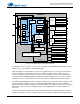
P.4.2 DSP Condenser
Cirrus Logic provides the customer with the DSP Condenser application to implement the design
capabilities described in Section P.1. The DSP Condenser application is the vehicle that allows system
designers to quickly program the CS4953x4/CS4970x4 DSP with the customer’s design and to access
Cirrus Logic powerful firmware suite.
See additional information about the DSP Condenser application in Chapter 8, "DSP Condenser".
P.5 CS40700x Pin Descriptions
P.5.1 Power and Ground
The following sections describe the CS4953x4/CS4970x4 power and ground pins. Decoupling and
conditioning of the power supplies is also discussed. Following the recommendations for decoupling and
power conditioning will help to ensure reliable performance.
P.5.1.1 Power
The CS4953x4/CS4970x4 Family of DSPs take two supply voltages — the core supply voltage (VDD) and
the I/O supply voltage (VDDIO). There is also a separate analog supply voltage required for the internal
PLL (VDDA). These pins are described in the following tables and descriptions.
The DSP Core supply voltage pins require a nominal 1.8V. The DSP I/O supply voltage pins require a
nominal 3.3V.
Table P-1. Core Supply Pins
LQFP-144
Pin #
LQFP-128
Pin #
Pin Name
Pin
Type
Pin Description
10 42 VDD1
Input
1.8V DSP Core supply.
This powers all internal logic and the
on-chip SRAMs and ROMs
24 55 VDD2
54 83 VDD3
66 95 VDD4
83 112 VDD5
98 125 VDD6
119 12 VDD7
130 22 VDD8
Table P-2. I/O Supply Pins
LQFP-144
Pin #
LQFP-128
Pin #
Pin Name
Pin
Type
Pin Description
18 50 VDDIO1
Input 3.3V I/O supply
33 62 VDDIO2
44 73 VDDIO3
60 89 VDDIO4
73 100 VDDIO5
91 120 VDDIO6
113 8 VDDIO7
136 28 VDDIO8