
User Manual

CS4953xx Data Sheet
32-bit Audio Decoder DSP Family
DS705F2 19
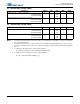
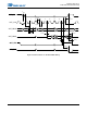
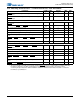
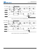
5.14 Switching Characteristics — Parallel Control Port - Intel Slave Mode
Parameter Symbol Min Typical Max Unit
Address setup before PCP_CS and PCP_RD low or PCP_CS and
PCP_WR
low
t
ias
5——ns
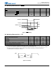
Address hold time after PCP_CS and PCP_RD low or PCP_CS and
PCP_WR
high
t
iah
5——ns
Read
Delay between PCP_RD then PCP_CS low or PCP_CS then
PCP_RD low
t
icdr
0——ns
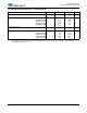
Data valid after PCP_CS and PCP_RD low
t
idd
— — 18 ns
PCP_CS and PCP_RD low for read
t
irpw
24 — — ns
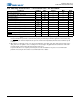
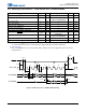
Data hold time after PCP_CS or PCP_RD high
t
idhr
8——ns
Data high-Z after PCP_CS or PCP_RD high
t
idis
— — 18 ns
PCP_CS or PCP_RD high to PCP_CS and PCP_RD low for next
read
1
1. The system designer should be aware that the actual maximum speed of the communication port may be limited by
the firmware application. Hardware handshaking on the PCP_BSY
pin/bit should be observed to prevent
overflowing the input data buffer. AN288 CS4953xx /CS497xxx Firmware User’s Manual should be consulted for
the firmware speed limitations.
t
ird
30 — — ns
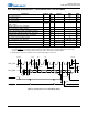
PCP_CS or PCP_RD high to PCP_CS and PCP_WR low for next
write
1
t
irdtw
30 — — ns
PCP_RD rising to PCP_IRQ rising
t
irdirqhl
— — 12 ns
Write
Delay between PCP_WR then PCP_CS low or PCP_CS then
PCP_WR low
t
icdw
0——ns
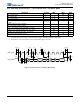
Data setup before PCP_CS or PCP_WR high
t
idsu
8——ns
PCP_CS and PCP_WR low for write
t
iwpw
24 — — ns
Data hold after PCP_CS or PCP_WR high
t
idhw
8——ns
PCP_CS or PCP_WR high to PCP_CS and PCP_RD low for next
read
1
t
iwtrd
30 — — ns
PCP_CS or PCP_WR high to PCP_CS and PCP_WR low for next
write
1
t
iwd
30 — — ns
PCP_WR rising to PCP_BSY falling
t
iwrbsyl
—2*DCLKP + 20— ns